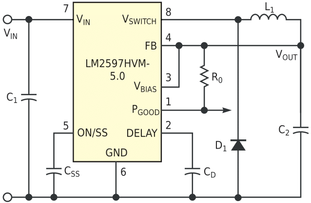
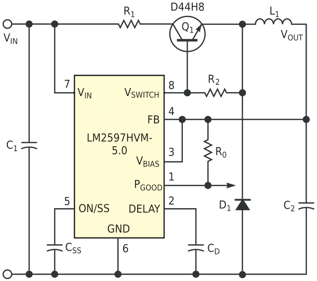
Industrial-control circuits often derive their power from widely varying sources that can exceed the 40 V maximum rating of popular switching ICs. This Design Idea presents a simple, flexible, and inexpensive buck switcher that converts an input voltage as high as 60 V to 5 V at several amps. The circuit is unique in that it boosts current with almost no compromise in performance, size, or cost. It should be of interest to anyone who has ever searched for a simple step-down switcher with an output current or input voltage exceeding that of off-the-shelf devices. Such a search usually entails a far more complex and costly solution than the one this Design Idea presents. LM2594HV and LM2597HV both feature 60 V maximum input, 150-kHz operation, 0.7 A peak output, and on/off capability. The 2597 adds soft start, delay, a power-good flag, and a pin you can use to bootstrap most of its bias current from VOUT. Although both devices are single-chip switchers, you can also use them as driver-controllers with only slight modifications to their standard buck-regulator circuit configurations. Figure 1 shows the 2597HVM in a typical 5 V, 0.5 A configuration that uses all the IC's features. Figure 2 shows the higher current configuration with only three additional components to boost output current to more than 6 A.
 |
|
| Figure 1. | This classic buck-regulator circuit efficiently steps down voltage. |
 |
|
| Figure 2. | You can increase output current more than tenfold with the addition of only three components. |
As a bonus, the circuit in Figure 2 also provides overcurrent and short-circuit protection for Q1. The rugged self-protection features of the IC also apply to Q1, provided that the transistor has sufficient heat sinking; L1 stays out of saturation if you select R1 properly. If the peak current in R1 produces a voltage drop large enough to cause Q1 to saturate, then the IC experiences an overcurrent condition, causing its internal protection modes either to disable the switch for the remainder of the pulse period or to skip pulses. Q1 needs to be a fast switch to minimize switching losses. The transistor also needs to have minimal storage time to avoid pulse skipping at low duty cycles. Table 1 shows circuit performance at its maximum input voltage, 60 V , under a variety of output conditions. The table also includes component values and ratings necessary to select sources for L1, C1, and C2.
| Table 1. | Efficiency versus output voltage and current. (Q1 – D44H8) | ||||||||||||||||||||||||||||||||||||||||||||||||||||||||||||||||||||||||||||||||||||||||||
|
|||||||||||||||||||||||||||||||||||||||||||||||||||||||||||||||||||||||||||||||||||||||||||
Efficiency for test conditions of VIN = 60 V and IOUT = 2 to 6 A measures 77% for VOUT = 5 V and rises to 87% for VOUT = 12 V. Efficiency is highest for the VIN range of 30 to 40 V, where its peak is 2% higher than the values in Table 1. Power dissipation is almost evenly divided among L1, D1, and Q1, so you should space these components to avoid hot spots and provide heat-sinking for as much as 3 W each at maximum current and voltage. A good layout should include lots of ground plane and short, wide traces on high-current paths. Output voltages other than 3.3, 5, and 12 V are also available by substituting the adjustable version of the 2597. This IC requires an added resistor pair from VOUT to the FB pin to ground. Calculate resistor-divider values to set the FB pin at 1.23 V for the desired output voltage. Although this design example uses the LM2597HVM-5.0, you can easily apply this current-boost technique using only three additional parts to any of buck devices, effectively extending their output-current capability more than tenfold. You need not use HV devices for applications with a maximum input voltage lower than 40 V.
The following seven steps provide a simplified procedure to select component values for a wide range of operating conditions, including those that Table 1 lists:
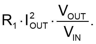
- Choose R1 to drop 1.5 V at the inductor's peak operating current of IOUT +20%. A higher current peak can force Q1 to saturate, causing the IC to deliver base current in excess of 0.7 A to Q1 This action triggers the IC's pulse-by-pulse current limit and protects the IC, Q1, and the load from further excessive current. An output short circuit causes the IC to reduce its clock frequency, protecting D1 and L1 from high continuous peak current. The power dissipated in R1, which can be a significant part of the total loss, subtracts from the dissipation in Q1, allowing for a smaller heat-sink requirement. This dissipation is:
- Choose R2 to be small enough to quickly turn off Q1 but not so small that it diverts much needed drive current away from Q1 and causes early current limit.
A value of 4.7 Ω (the value that Table 1 uses) is a good trade-off value for most applications. - Choose Q1 to be a fast switch with VCE rating greater than 60 V and ICE rating of two times the desired current peak. This ratio generally provides a high beta over the working-current range. The D44H8 works well to more than 6 A output in a TO-220 package and more than 2 A in an SOT-223 package.
- Choose D1 to be a Schottky diode rated for the maximum values of VIN and IOUT. D1 dissipates much of the total power loss when VIN >> VOUT, so look for a diode rated at less than 0.5 V forward drop.
- Choose L1 = 47 µH/√IOUT for VOUT = 3.3 V, 68 µH/√IOUT for VOUT = 5 V and 150 µH/√IOUT for VOUT = 12 V. Choose the nearest L1 value with a saturation and working current rating greater than IOUT. Coilcraft's SMT DO5022 family works well for output current to 1 or 2 A, but you need larger cores for currents greater than 3 A. You can tie these SMT inductors in series or in parallel to extend their use to 3 to 4 A. They're also available in stacked-core versions for higher current use. Through-hole inductors, such as Coilcraft's DMT2-xx family, are physically larger but provide lower losses, especially for output current greater than 5 A.
- Choose C1 for ripple-current rating and C2 for low ESR. A minimum capacitance value for C1 = C2/10 ≥ 100 µF × IOUT works well at low current, but, as current rises to several amps, you need larger values to meet ESR and ripple-current requirements. Ripple-current rating depends on several variables, but a conservative choice is half the maximum output current for C1 and one-fourth the maximum output current for C2. High ripple-current capability may require paralleling several capacitors for C1 Select C2 to have ESR less than 0.1 Ω/IOUT to keep the VOUT peak-to-peak ripple less than 50 mV. Choose capacitors by looking at those targeting high-temperature use in switching power supplies with published ESR and ripple current ratings. Then, select a voltage rating higher by at least 50% than the expected operating voltage.
- R0, CSS, and CD are optional. You can leave these pins open if you don't intend to use them. You can shut off the circuit by pulling Pin 5 low and then turn it on again with soft-start by allowing Pin 5 to float high. Refer to the 2597 data-sheet graphs for CSS and CD values necessary to set the desired soft-start and power-good flag delay times.