A DC load is an essential testing tool for any electronic enthusiast, especially for testing and repairing power supplies. An adjustable DC load can limit the current at any desired level, which makes it suitable to perform various tests because some problems of the feedback loop are only detectable by variable load tests. Also for any SMPS repair attempt, the output should be tested against some loads, not just voltage stability, because the problem might lie within the current sensing on the primary side (a common problem of Flyback SMPSs).
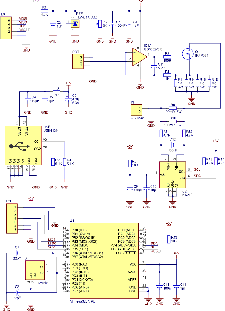
This article introduces a digital DC load with a 1.54-inch OLED display to read the load’s voltage, current, and power values simultaneously. An accurate Texas Instrument zero-drift SOT23-8 INA219 current sensing chip reads the voltage and current values and sends the data through an I2C bus to the ATmega328 microcontroller. The microcontroller makes the calculations and displays the parameters on an SSD1309 128×64 1.54-inch OLED display. The interface between the MCU and display is HW SPI. A zero-drift rail-to-rail input-output opamp such as the GS8552-SR and some passive components enhance the stability of the CC circuit. The reference voltage of the opamp has been stabilized using a TL431 shunt regulator.
The schematic and PCB have been designed using Altium Designer 24 and the Gerber files are available to download from the Downloads section. You can power the board using your mobile phone USB Type-C charger; no external power supply is necessary.
Circuit analysis
Figure 1 shows the schematic diagram of the dc load. The current sensing chip is INA219 and the microcontroller is ATMega328.
 |
|
| Figure 1. | Schematic diagram of the 5 A adjustable digital DC load. |
According to the datasheet, INA219 is an interesting chip to read the current: “The INA219 is a current shunt and power monitor with an I2C- or SMBUS-compatible interface. The device monitors shunt voltage drop and bus supply voltage, with programmable conversion times and filtering. A programmable calibration value and an internal multiplier enable direct current readouts in amperes. An additional multiplying register calculates power in watts. The I2C- or SMBUS-compatible interface features 16 programmable addresses. The INA219 is available in two grades: A and B. The B-grade version has higher accuracy and higher precision specifications. The INA219 senses across bus shunts varying from 0 to 26 V. The device uses a single 3- to 5.5-V supply, drawing a maximum of 1 mA supply current. The INA219 operates from –40 °C to 125 °C.”
USB is a USB4135 connector to easily power the board using a typical USB Type-C cable. R2 and R4 are pulldown resistors to indicate the USB connector is on the “load side”, but because the current consumption of the circuit is low, not mounting these resistors won’t affect the board’s operation. FB (1206 ferrite bead) and C4 … C6 reduce the USB-V noise.
R1 and C3 build a low pass filter because the reference input voltage to the CC circuit should be as noise-free as possible. REF is the TLV431A shunt regulator chip to stabilize the reference voltage of the CC circuit within the operational temperature range. The output voltage of this shunt is around 1.25 V. R3 adjusts the voltage to the POT (1K potentiometer) to provide a wider turning course for the POT because the POT input voltage defines the maximum CC current (for smooth current adjustment).
C7 and C8 are decoupling capacitors for IC1. IC1 is the GS8552 zero-drift rail-to-rail input-output opamp to run the CC circuit sustainably (IC1, Q1, R7, R8, C11, R11, R14, R16, R18). According to its datasheet, Q1 is the IRFP064 MOSFET that could handle currents up to 70 A (25 °C, VGS = 10 V). R11, R14, R16, R18 resistors must be rated at 3 W each.
IN is the board’s input terminal (25 Vmax). R9 and R10 build a single 6 W 0.05R shunt resistor (two 3 W-0.1R resistors in parallel). The maximum power dissipation on these resistors is 1.25 W at the maximum 5 A current (0.05R × 5 A × 5 A). The power rating of the shunt could be increased to 8 W (2 × 0.1R-4 W), however, the cost of such resistors would be higher. R6, R12, and C12 differentially reduce the noise and spikes on the voltage-sensing path. IC2 is the INA219 zero-drift bi-directional 0.5%-error current sensing chip that reads the voltage and current values and sends the data to U1. R15 and R17 are mandatory pull-up resistors on the I2C bus. R5, C9, and C10 build a low-pass filter to reduce the input noise to IC2.
U1 is the ATMega328 microcontroller that reads the I2C data and displays the values on the OLED (LCD 7Pin XH connector). The controller chip of the OLED display is SSD1309 and the communication type is HW SPI. CS, DC, and RST pins are defined programmatically in the code.
C13 and C14 are decoupling capacitors for U1 and X is a 3225 12 MHz SMD crystal to provide the clock source for the microcontroller. R13 is a pull-up resistor for the RESET pin of the microcontroller to avoid any unwanted reset trigger and instability. ISP is a 2.54 mm male pin header that provides an AVR-ISP programming interface for the microcontroller (GND-RST-MISO-MOSI-SCK).
PCB layout
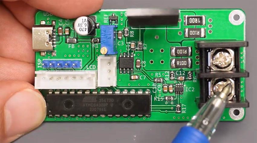
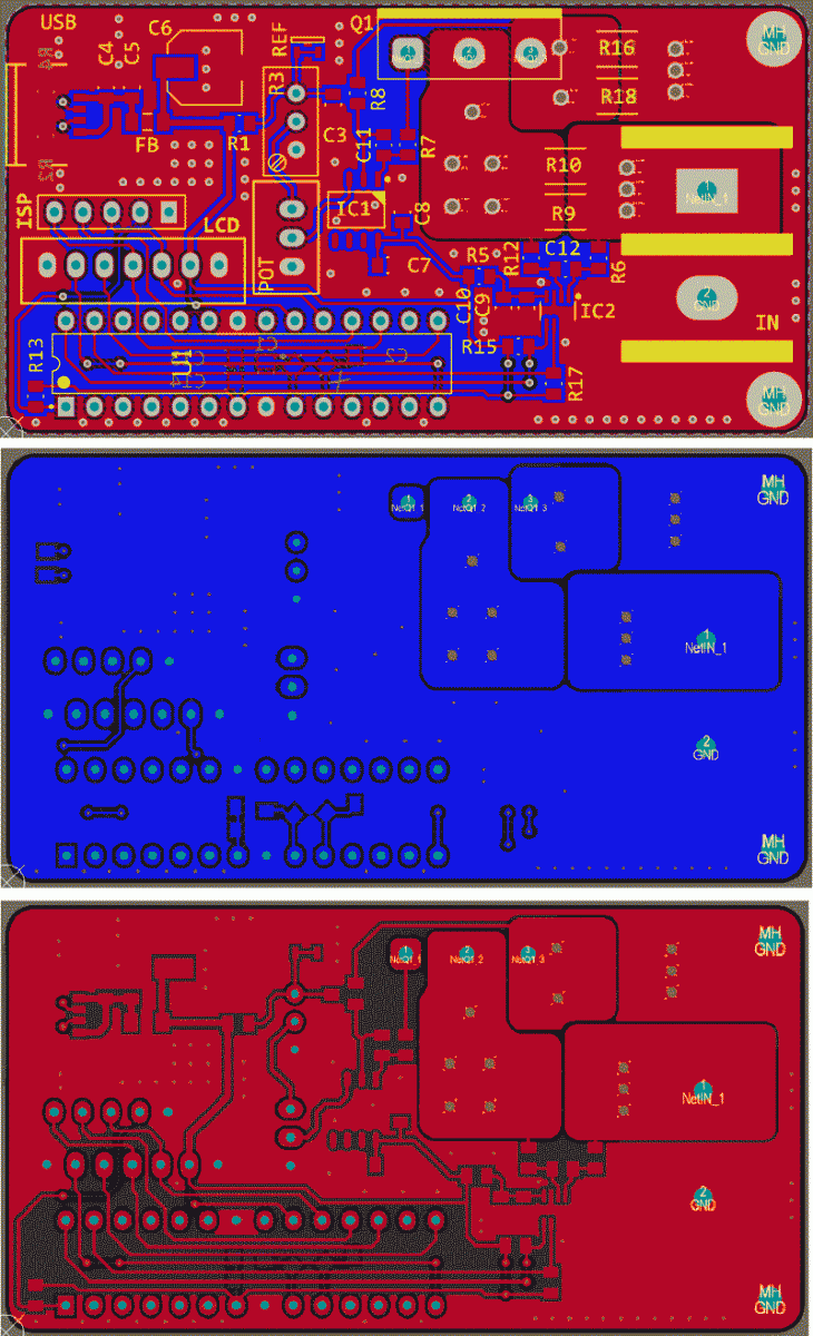
Figure 2 shows the PCB layout of the design. It’s a two-layer PCB board and contains a mixture of SMD and through-hole components.
 |
|
| Figure 2. | PCB layout of the 5 A adjustable digital DC load circuit. |
Some parts of the PCB and a few PCB nets should carry currents up to 5 A (input terminal, shunt, MOSFET pins). That’s why these high-current carrying PCB nets have been implemented using VIA-snitched double-layer copper planes. This technique reduces the copper resistance significantly and allows the copper to pass the current without a significant temperature increase.
The PCB has been divided into several regions: Type-C input and power supply, digital and microcontroller, power MOSFET, and input terminal. This is the most important factor in all PCB designs, from simple to complex mixed-signal. Ground polygon planes and vias reduce the ground impedance and length of the ground path, bringing less noise and higher stability. Placing vias near the ground pin of decoupling capacitors is a good practice.
 |
|
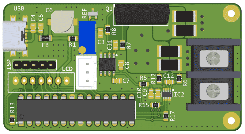
| Figure 3. | Assembly drawing of the PCB board. |
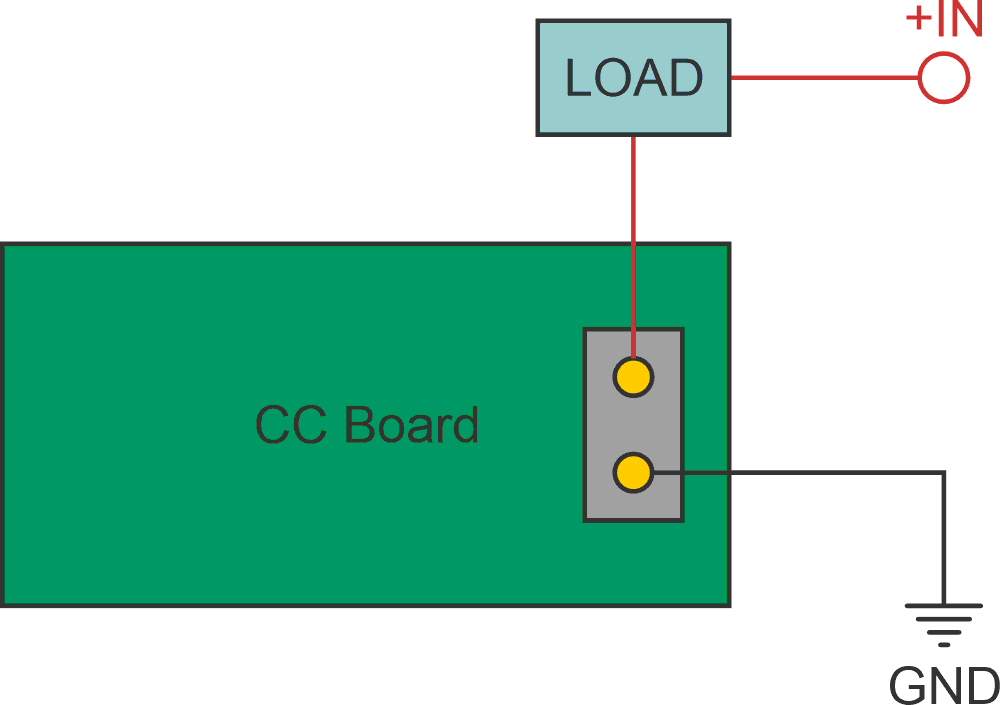
Figure 3 shows the assembly drawing of the PCB board. Follow Figure 4 to connect your load to the DC load. PCB files and MCU code are available for download from the Downloads section.
 |
|
| Figure 4. | Wiring diagram of input power, your load, and CC DC load. |