This page provides a detailed explanation of how the modified cascode light receiver circuit operates. The cascode technique in conjunction with an inductive load provides very high current to voltage conversion as well as very high speed.
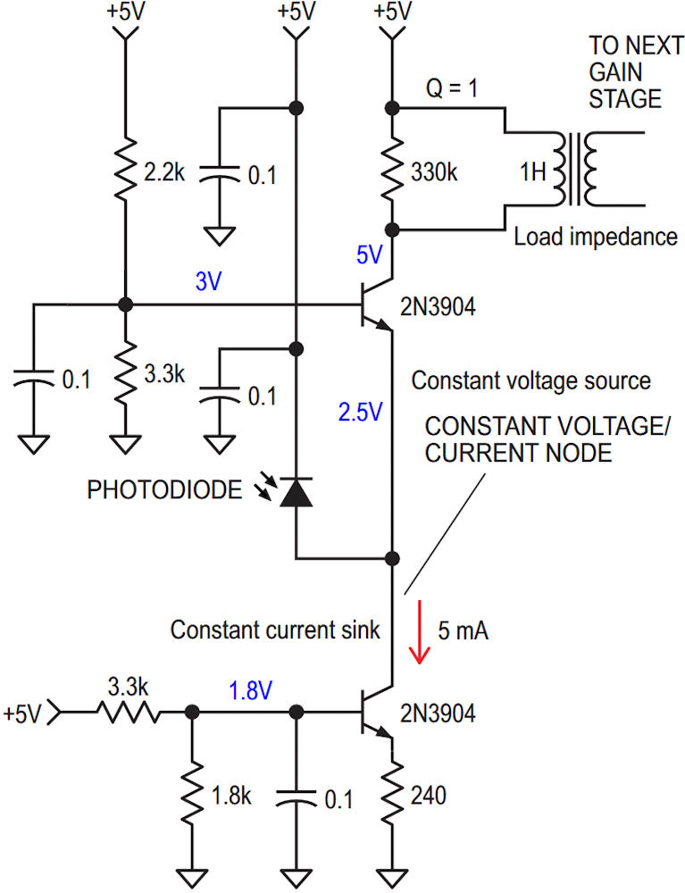
Upper NPN transistor forms an emitter follower constant voltage source. Bottom NPN transistor forms a constant current sink.
The junction where the two circuits meet tries to keep the voltage and current constant.
Current changes fed into the node show up as current changes through the upper transistor collector load impedance.
The current from the photo diode is added to the node. Since the current is held constant by the bottom circuit, any additional current fed into the node will result in a current reduction through the upper transistor load impedance.
If
ID = photodiode current,
IA = upper NPN load current,
IB = lower NPN current,
then IB = IA + ID or IA (load) = IB – ID
The circuit does not produce any current or voltage gain, it isolates the load from the PIN photo diode. PIN photo diode current is translated into the load impedance.
Since the node voltage is held constant, the voltage across the photo diode is also fixed. The diode’s capacitance effect on speed is therefore minimized.
With an inductive load, only current changes will produce a voltage drop across the impedance. Ambient light induced current from the photo diode will not produce a voltage across the inductive load. However, the photo diode current must not be high enough to exceed the bottom NPN current sink level.
The resistor in parallel with the inductor is used to keep the Q of the circuit limited. For a wide bandwidth the Q should be held to a value of one or less.