The circuit presented here is a 3 W stereo audio amplifier with memory UP/DOWN volume control. The project is based on PAM8408 IC from Diode Incorp which is a filter-less class-D amplifier with high SNR and Differential input which helps eliminate noise.
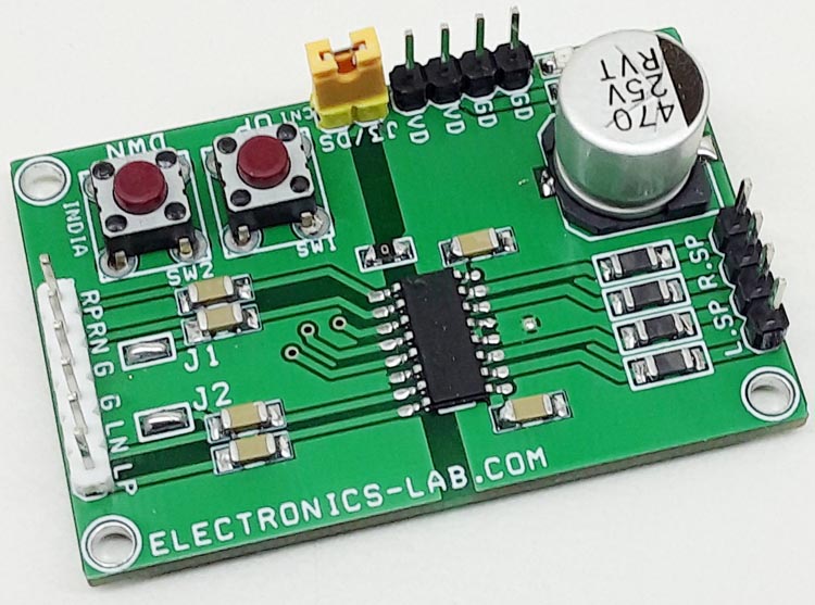
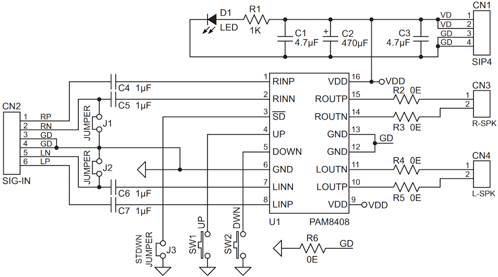
The circuit presented in Figure 1 is a 3 W stereo audio amplifier with memory UP/DOWN volume control. The project is based on PAM8408 IC from Diode Incorp which is a filter-less class-D amplifier with high SNR and Differential input which helps eliminate noise. Two tactile switches are provided to control the UP/DOWN volume in 32-steps and it will hold the setting when the chip is in shutdown mode. The operating supply is 2.5 V to 6 V DC and this supply range helps to operate it with batteries like the use of 4 × Alkaline batteries. The small PCB size, 87% efficiency, low cost, minimum external components make this project ideal for portable applications.
 |
|
| Figure 1. | Schematic diagram of a class-D amplifier. |
The PAM8408 also has built-in auto-recovery SCP (Short Circuit Protection) and thermal shutdown. The circuit works with differential audio signal input. It is advisable to use shielded wire for the audio input signals. Jumper J3 is open in normal operation, and if you close it puts the amplifier into shutdown mode and the audio volume will memorize when shutdown mode is recovered. Solder jumpers J1 and J2 are optional and of no use, it is advisable to keep these jumpers open. Connector CN1 is for power supply, CN2 is for audio signal input, CN3, and CN4 are for the speaker, jumper J3 is for shutdown, D1 is the power LED, Switch 1 increased volume, and Switch 2 decreases volume.
Volume changes are affected by toggling either the UP or DOWN tactile switches. After a period of 1 cycle pulses with either the UP or DOWN switch press, the volume will change to the next specified step, either UP or DOWN, and followed by a short delay. This delay decreases the longer the line is held low, eventually reaching a delay of zero. The delay allows the user to pull the UP or DOWN terminal low once for one volume change, or hold down to ramp several volume changes. The delay is optimally configured for push-button volume control. If either the UP or DOWN pin remains low after the first volume transition the volume will change again, but this time after 10 cycles. The followed transition occurs at 4 cycles for each volume transition. This is intended to provide the user with volume control that pauses briefly after initial application, and then slowly increases the rate of volume change as it is continuously applied. There are 32 discrete gain settings ranging from +24 dB as maximum to –80 dB as a minimum. Upon device power on, the amplifier’s gain is set to a default value of 12 dB, and the gain will remain when Shutdown Jumper J3 is closed.
Features
- Operating power supply 5 V (2.5 V to 6 V range)
- 2 × 3 W power output 4 Ohms speaker @ 10% THD
- Fully differential audio signal input for low noise operations
- Onboard shutdown jumper J3
- D1 power LED
- Ferrite bead on outputs for low EMI
- 32-step memory up/down volume control from –80 dB to 24 dB
- Low THD+N
- Superior low noise: 60 µV
- Minimize pop/clip noise
- Auto recovery short circuit protection
- Thermal shutdown
- PCB dimensions 49.53 × 32.54 mm
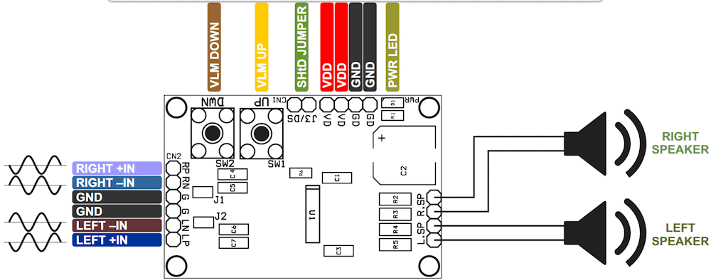
Figure 2 shows the amplifier connection diagram.
 |
|
| Figure 2. | The class-D amplifier connection diagram. |
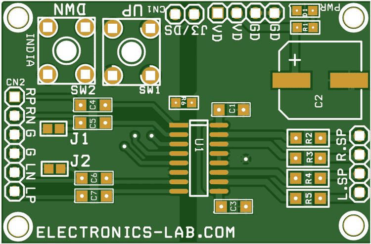
The Gerber project files can be downloaded from the link in the Downloads section. The PCB layout is shown in Figure 3. Table 1 shows the bill of materials.
 |
|
| Figure 3. | The PCB layout. |
| Table 1. | List of circuit components | |||||||||||||||||||||||||||||||||||||||
|
||||||||||||||||||||||||||||||||||||||||