NXP NTAG I2C solution enables feature-rich options on home appliances and wearable devices – as well as ability to power itself
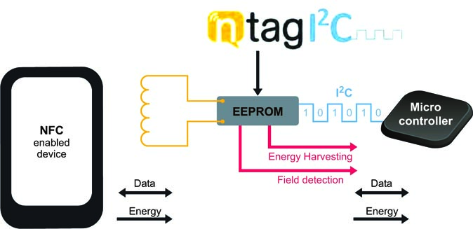
 NXP Semiconductors announced a complete passive solution for near field communication (NFC) interaction for a wide variety of applications such as home appliances, consumer electronics, wearable technology and home automation. By combining a contactless NFC interface with a contact I²C interface and onboard non-volatile memory, the NTAG I²C solution enables new kinds of NFC tag interactions, including advanced device pairing, personalization of electronic devices, and device maintenance. While existing NTAG solutions can only interact with NFC-enabled devices, the new NTAG I²C memory can be accessed via the existing embedded microcontroller of any electronic device.
“The NTAG I²C is the most complete solution for passive NFC interactions, taking NFC beyond its traditional ecosystem and allowing an exciting new range of applications. Using NTAG I²C, appliance manufacturers and wearable device makers can offer feature-rich options to consumers, allowing them to use their existing NFC-enabled mobile phones as a remote user interface, rather than relying on expensive touchscreens or Wi-Fi connectivity for wireless data exchange on home electronics,” said Rutger Vrijen, vice president and general manager, tagging and infrastructure business line, NXP Semiconductors. “It will now become possible to use the highly intuitive UI on your smartphone to program a washing machine, exchange data with an exercise bike or wristband, and download specific cooking recipes to your microwave oven.”
Optimized for very low-power operation, the passive NTAG I²C solution is capable of energy harvesting from the mobile device to power external circuitry such as low power microcontrollers. It also includes a field-detect function for automatic power-up, so that the mobile device’s battery is not drained during standby while waiting for a NFC phone. As the first fully ISO 14443A / NFC Forum Compliant Type 2 Tag chip with I²C interface and energy harvesting with on board EEPROM, the NTAG I²C solution ensures compatibility with all NFC-enabled devices and allows data to be saved even if the power supply is lost. These features combined make the NTAG I²C particularly well suited for the configuration, calibration or customization of wearable devices.
The new NTAG I²C features a specific pass-through mode, which allows the device to serve as an easy to integrate communication pipe for unlimited bi-directional data exchange between the feature-rich NFC device, which may have a connection to the cloud and an advanced user-interface/display, and the electronic devices. The new device is also fully supported by the recently released MIFARE SDK (Software Development Kit). Designed to provide access to all hardware features on Java level, the MIFARE SDK streamlines the development of Android apps to interact with NTAG devices. The SDK allows Android app developers to concentrate efforts on designing creative apps for a wide range of new applications that support the Internet of Things (IoT) and wearable technology.
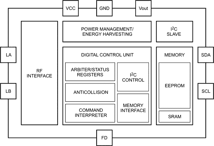 |
| NTAG I2C block diagram. |
Key Features and Benefits of the NTAG I²C Solution:
- RF Interface
- Fully compliant with ISO/IEC 14443A
- Fully compliant with NFC Forum Type 2 Tag
- Input capacitance of 50 pF, reducing coil size and lowering BOM/antenna footprint
- Contact Interface
- I²C interface supports standard (100 kHz) and fast (400 kHz) modes
- Memory
- 888 or 1,904 bytes of user memory for NDEF message or data storage (based on EEPROM)
- Read-only locking function
- Identification
- Unique 7-byte serial number to help validate authenticity
- Get Version command for easy identification of chip type and supported features
- Data transfer
- 64-byte SRAM memory buffer enabling efficient “pass-through” of data, not limited by EEPROM memory cycles and using field detection signal as a mean of data transfer synchronization
- Clear arbitration between RF and I²CFast Read command for shorter test times and increased throughput
- Low power operations
- Non-volatile storage of data for zero power configuration
- Configurable Field Detect output signal to facilitate automatic power-up, while eliminating the need for software polling
- Energy harvesting to provide sufficient power to drive a low-power microcontroller, LEDs and other circuitry (e.g. for sensors)