Analog Devices today introduced a pair of highly integrated precision analog microcontrollers featuring on-chip memory, data converters, and other analog peripherals that combine to deliver the highest level of programmability and smallest package size. Effective for digital diagnostics in optical transceivers and modules based on both fixed and tunable frequency lasers, the ADuC7023 and ADuC7122 precision analog microcontrollers use an ARM7 processor with up to 126 KB of flash memory to ensure the accurate control of optical drivers and diagnostics.
The new microcontrollers feature on-chip 12-bit ADCs (analog-to-digital converters) and DACs (digital-to-analog converters), which reduce the size of the overall solution by up to 75 percent compared to competing discrete solutions. The devices support interrupt nesting and up to 16 levels of interrupt priority, and retain DAC and GPIO outputs during a software or watchdog reset, which are of particular benefit to optical module designers.
ADuC7122 Analog Microcontroller Boosts Control Functions in Tunable Optical Modules
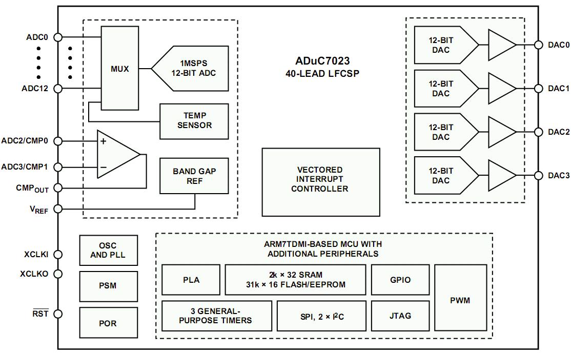
The ADuC7122 is a fully integrated, 1 MSPS, 12-bit data acquisition system, incorporating high performance multichannel ADCs, 12 voltage output DACs, 16-bit/32-bit MCUs, and Flash/EE memory on a single chip. The ADC consists of up to 13 inputs. Four of these inputs can be configured as differential pairs with a Programmable Gain Amplifier on their front end providing a gain between 1 and 5. The ADC can operate in single-ended or differential input modes. The ADC input voltage is 0 V to VREF. A low drift band gap reference, temperature sensor, and supply voltage monitor complete the ADC peripheral set.
The DAC output range is programmable to one of two voltage ranges. The DAC outputs have an enhanced feature of being able to retain their output voltage during a watchdog or software reset sequence.
The devices operate from an on-chip oscillator and a PLL, generating an internal high frequency clock of 41.78 MHz. This clock is routed through a programmable clock divider from which the MCU core clock operating frequency is generated. The microcontroller core is an ARM7TDMI®, 16-bit/32-bit RISC machine that offers up to 41 MIPS peak performance. Eight kilobytes of SRAM and 126 kilobytes of nonvolatile Flash/EE memory are provided on chip. The ARM7TDMI core views all memory and registers as a single linear array.
The ADuC7122 contains an advanced interrupt controller. The vectored interrupt controller (VIC) allows every interrupt to be assigned a priority level. It also supports nested interrupts to a maximum level of eight per IRQ and FIQ. When IRQ and FIQ interrupt sources are combined, a total of 16 nested interrupt levels are supported.
On-chip factory firmware supports in-circuit download via the I2C serial interface port, while nonintrusive emulation is also supported via the JTAG interface. These features are incorporated into a low cost QuickStart™ Development System supporting this MicroConverter® family. The part contains a 16-bit PWM with six output signals.
For communication purposes, the part contains 2 × I2C channels that can be individually configured for master or slave mode. An SPI¯ interface supporting both master and slave modes is also provided.
The parts operate from 3.0 V to 3.6 V and are specified over atemperature range of −10°C to +95°C. The ADuC7122 is available in a 108-Ball BGA package.
ADuC7023 Analog Microcontroller for Fixed Frequency Laser Applications
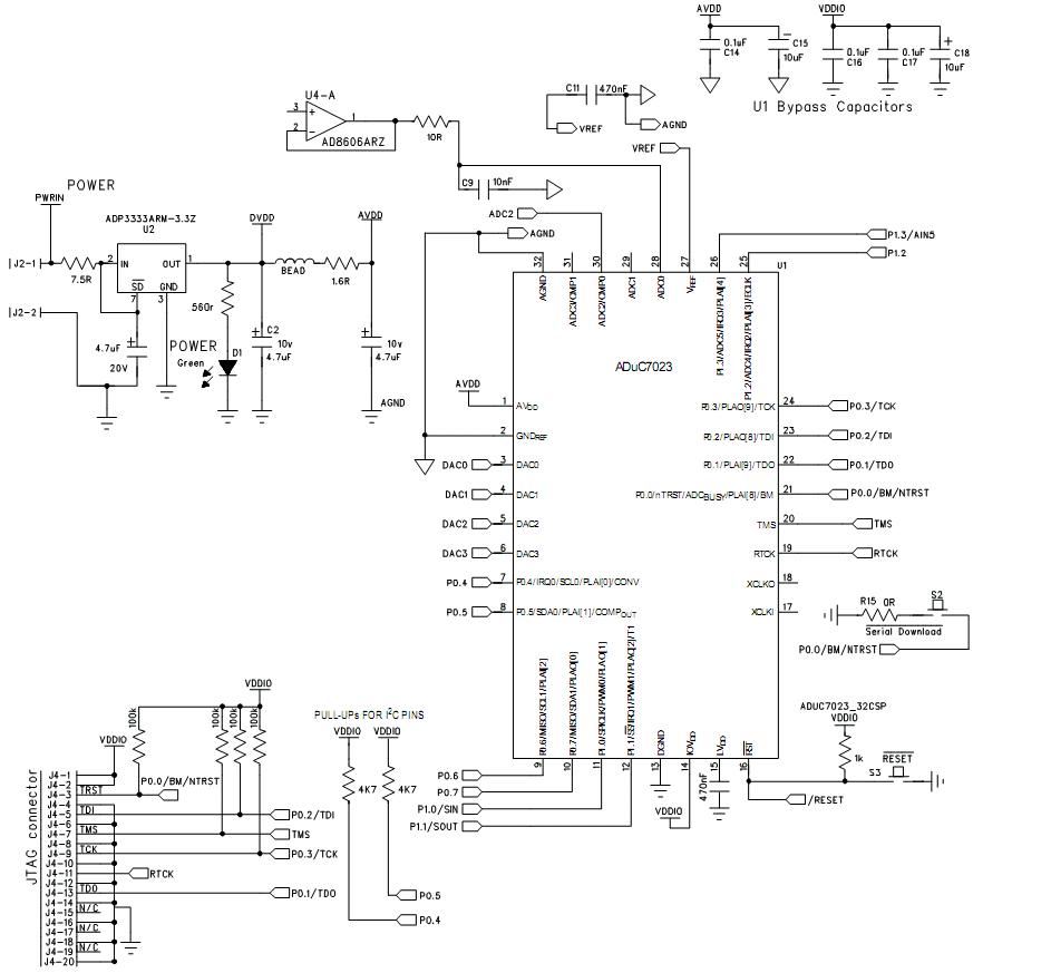
The ADuC7023 is a fully integrated, 1 MSPS, 12-bit data acquisition system, incorporating high performance multichannel ADCs, 16-bit/32-bit MCUs, and Flash/EE memory on a single chip. The ADC consists of up to 12 single-ended inputs. An additional four inputs are available but are multiplexed with the four DAC output pins. The ADC can operate in single-ended or differential input modes. The ADC input voltage is 0 V to VREF. A low drift band gap reference, temperature sensor, and voltage comparator complete the ADC peripheral set. The DAC output range is programmable to one of two voltage ranges. The DAC outputs have an enhanced feature of being able to retain their output voltage during a watchdog or software reset sequence.
The devices operate from an on-chip oscillator and a PLL, generating an internal high frequency clock of 41.78 MHz. This clock is routed through a programmable clock divider from which the MCU core clock operating frequency is generated. The microcontroller core is an ARM7TDMI®, 16-bit/32-bit RISC machine that offers up to 41 MIPS peak performance. Eight kilobytes of SRAM and 62 kilobytes of nonvolatile Flash/EE memory are provided on chip. The ARM7TDMI core views all memory and registers as a single linear array. The ADuC7023 contains an advanced interrupt controller. The The ADuC7023 is a fully integrated, 1 MSPS, 12-bit data acquisition system, incorporating high performance multichannel ADCs, 16-bit/32-bit MCUs, and Flash/EE memory on a single chip.
The ADC consists of up to 12 single-ended inputs. An additional four inputs are available but are multiplexed with the four DAC output pins. The ADC can operate in single-ended or differential input modes. The ADC input voltage is 0 V to VREF. A low drift band gap reference, temperature sensor, and voltage comparator complete the ADC peripheral set. The DAC output range is programmable to one of two voltage ranges. The DAC outputs have an enhanced feature of being able to retain their output voltage during a watchdog or software reset sequence. The devices operate from an on-chip oscillator and a PLL, generating an internal high frequency clock of 41.78 MHz. This clock is routed through a programmable clock divider from which the MCU core clock operating frequency is generated. The microcontroller core is an ARM7TDMI®, 16-bit/32-bit RISC machine that offers up to 41 MIPS peak performance. Eight kilobytes of SRAM and 62 kilobytes of nonvolatile Flash/EE memory are provided on chip. The ARM7TDMI core views all memory and registers as a single linear array.
The ADuC7023 contains an advanced interrupt controller. The vectored interrupt controller (VIC) allows every interrupt to be assigned a priority level. It also supports nested interrupts to a maximum level of eight per IRQ and FIQ. When IRQ and FIQ interrupt sources are combined, a total of 16 nested interrupt levels are supported. On-chip factory firmware supports in-circuit download via the I2C serial interface port, and nonintrusive emulation is supported via the JTAG interface. These features are incorporated into a low cost QuickStart™ development system supporting this MicroConverter® family. The part contains a 16-bit PWM with five output signals.