By Charly El-Khoury, Analog Devices
This article shows how compensating an amplifier - such as the ADA4895-2, which is normally stable for a gain higher than +9 -to operate with a gain as low as +2 provides higher slew rate and faster settling time than an equivalent internally compensated amplifier. Two methods will be presented, and advantages and disadvantages of each circuit will be highlighted.
The ADA4895-2, a device in the same family as the ADA4896-2, ADA4897-1, and ADA4897-2, is a dual low-noise, high-speed, voltage-feedback amplifier with rail-to-rail outputs. Stable with a minimumgain of 10, it features 1.5-GHz gain-bandwidth product, 940-V/µs slew rate, 26-ns settling time to 0.1%, 2-nV/√Hz 1/f noise at 10 Hz, 1-nV/√Hz wide band noise, and −72-dBc spurious-free dynamic range at 2 MHz. Operating with a 3-V to 10-V supply, it draws a quiescent current of 3 mA per amplifier.
 |
|
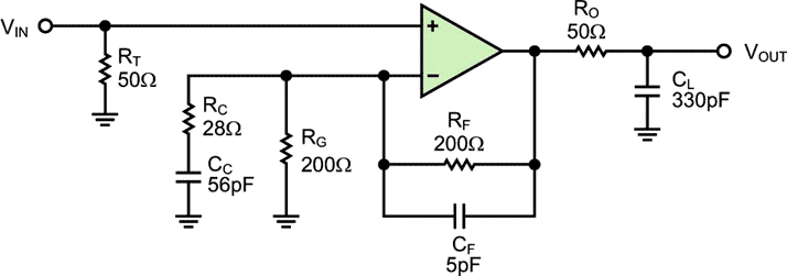
| Figure 1. | Method 1: Compensating the ADA4895-2 for a stable gain of +2. |
Method 1, shown in Figure 1, adds a simple RC circuit (RC = 28 Ω and CC = 56 pF) to the inverting input and a feedback capacitor (CF = 5 pF) in parallel with the feedback resistor. The circuit has a noise gain of +9 at high frequencies and a gain of +2 at frequencies below the resonance frequency, 1/2πRCCC = 100 MHz. Even though the noise gain at higher frequencies is approximately +9, the total output noise can be kept low as long as the low-pass filter, formed with RO and CL, blocks the high-frequency content. This allows the amplifier to operate at a gain of +2 while keeping the total output noise very low (3.9 nV/√Hz).
This configuration is scalable to accommodate any gain between +2 and +9. Table 1 shows the component values and total wideband output noise for each gain setting.
| Table 1. | Component Values Used for Gain < +10. RT = RO = 49.9 Ω. |
| Gain | RC (Ω) |
CC (pF) |
RG (Ω) |
RF (Ω) |
CL (pF) |
Total Output Noise (nV/√Hz) |
| +2 | 28.6> | 56 | 200 | 200 | 330 | 3.88 |
| +3 | 33.3 | 56 | 100 | 200 | 270 | 5.24 |
| +4 | 40 | 56 | 66.7 | 200 | 200 | 6.60 |
| +5 | 50 | 56 | 50 | 200 | 150 | 7.96 |
| +6 | 66.7 | 40 | 40 | 200 | 150 | 9.32 |
| +7 | 113 | 30 | 37.5 | 226 | 120 | 10.82 |
| +8 | 225 | 20 | 32.1 | 226 | 120 | 12.18 |
| +9 | — | — | 31.1 | 249> | 100 | 13.67 |
 |
|
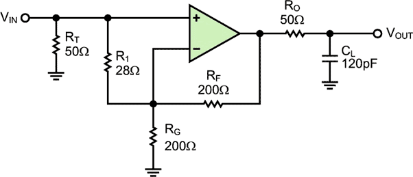
| Figure 2. | Method 2: Compensating the ADA4895-2 for a stable gain of +2. |
Method 2, shown in Figure 2, adds a resistor (R1 = 28 Ω) between the inverting and noninverting inputs to increase the amplifier’s noise gain to +9. No voltage appears across R1, so no current flows through it. Thus, the input impedance looking into R1 in parallel with the noninverting input will remain high. The input-to-output signal gain is equal to 1 + RF/RG, or +2 in this case. No capacitor is used in the compensation circuit, so there is no frequency dependency. This means that the wideband output noise is always higher at lower frequencies as compared to the first method.
This configuration is also scalable to accommodate any gain between +2 and +9. Table 2 shows the component values and total wideband output noise for each gain setting.
| Table 2. | Component Values Used for Gain < +10. RT = RO = 49.9 Ω, CL = 120 pF. |
|
Gain
|
R1
(Ω) |
RG
(Ω) |
RF
(Ω) |
Total Output Noise
(nV/√Hz) |
|
+2
|
28.6
|
200
|
200
|
13.39
|
|
+3
|
33.3
|
100
|
200
|
13.39
|
|
+4
|
40
|
66.5
|
200
|
13.39
|
|
+5
|
49.9
|
49.9
|
200
|
13.39
|
|
+6
|
66.5
|
40
|
200
|
13.39
|
|
+7
|
113
|
37.4
|
226
|
13.53
|
|
+8
|
225
|
32.4
|
226
|
13.53
|
|
+9
|
—
|
30.9
|
249
|
13.67
|
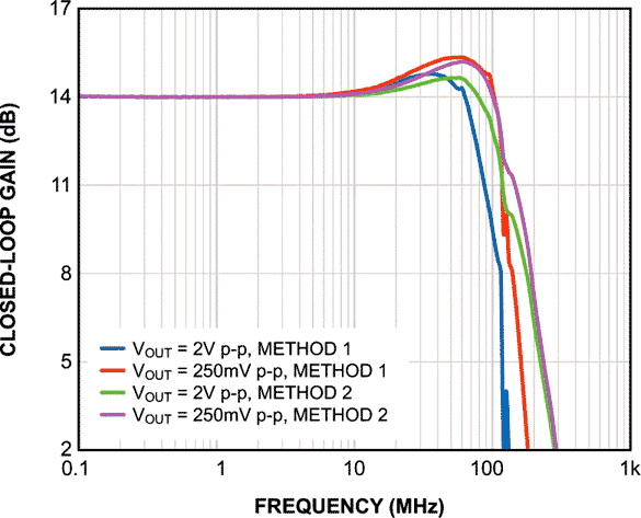
Figure 3 shows the small signal and large signal frequency responses of the circuits shown in Figure 1 and Figure 2 into a 50-Ω analyzer, with G = +5 V/V or 14 dB. As shown, both circuits are very stable, and the peaking is a little over 1 dB. This stability will apply throughout the range of gains between +2 and +9 as long as the values in Table 1 and Table 2 are used.
 |
|
| Figure 3. | Frequency response for G = +5. |
For better total output noise, the low-pass RC filter at the output can be adjusted to cut the bandwidth of this circuit at 50 MHz or below, depending on the application.
Why the Output Noise Is Better in Method 1 as Compared to Method 2
The output noise of Method 1 is much lower than that of Method 2, especially at gains below +7, because the noise gain of Method 1 is only high at high frequencies. At this point, a low-pass filter can be used to eliminate the high-frequency noise content. In Method 2, on the other hand, the amplifier is always operating at a noise gain of +9, even at low frequencies. Thus, the total output noise does not vary with the gain, as shown in Table 2.
Advantages and Disadvantages of Each Method
We have shown two different methods, using a few external components, to make an amplifier that is designed for stability at higher gains operate stably at lower gain. Method 1 uses more passive components, which can increase board space and add cost as compared to Method 2. In return, the total output noise of the first circuit is lower than that of the second circuit. Therefore, the circuit choice will be determined by the application and its required specifications.
 |
|
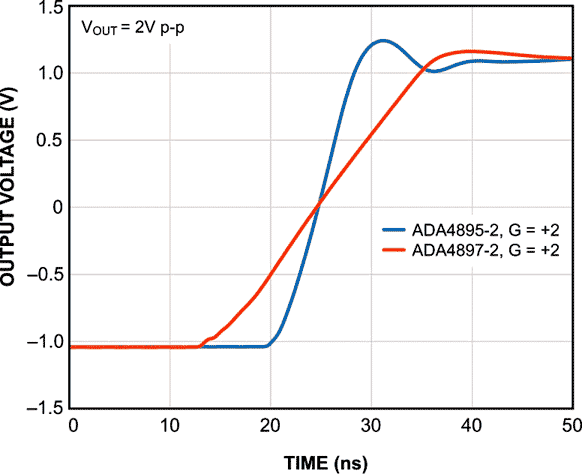
| Figure 4. | Comparing the compensated and decompensated amplifiers at G = +2. |
As shown in Figure 4, the decompensated ADA4895-2 provides a higher slew rate (300 V/µs vs. 100 V/µs) and faster settling time as compared to the internally compensated ADA4897-2, which is stable for gains ≥ +1. These advantages increase as the circuit gain increases.
Conclusion
A decompensated amplifier, such as the ADA4895-2, which is stable for G ≥ +10, can be compensated to allow operation at lower gains. The two methods presented here trade complexity for total wideband noise. Both provide higher slew rate and faster settling time than the equivalent internally compensated ADA4897-2, which is stable for G ≥ +1.