Chin-Leong Lim, Avago Technologies
Electronic Design
Front-end limiter circuits using Schottky and PIN diodes can provide needed protection in communications and other RF systems. However, designers still must deal with the upper-frequency limit problem. Synchronous or asynchronous transmissions can overload the front end of a wireless communication receiver. In time-domain duplexed systems, imperfect isolation between ports of a switch or a circulator is responsible for synchronous overload, whereas the asynchronous overload arises from unintended coupling between co-located aerials of unrelated systems.
The situation is different in nuclear magnetic resonance (NMR) receivers, where another cause of overloading is the ringing from the probe coil’s stored energy following the stimulus pulse. The shrinking device size of low-noise amplifiers (LNAs) to improve RF performances unfortunately trades off the overload immunity. For example, the maximum input power (PiMAX) ratings for 400-µm and 800-µm LNA devices in 0.25-µm pseudomorphic high electron mobility transistor (PHEMT) technology are 7 dBm and 10 dBm, respectively.
Overloading also adversely affects hardware and information integrity. Large overdrive leads to immediate device failure, which occurs when the bond-wires/metallization fuse or when the transistor junction suffers melt down. The exponential increase in gate current with overdrive also shortens device lifetime because of metal migration. Chronic exposure to small overload can degrade either the device’s output power or third-order output intercept point. As a consequence, NMR receivers lose critical information during the “dead-time” period while the front end gradually recovers from saturation.
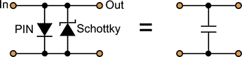
A limiter prevents overload by allowing RF signals that are below a certain threshold to pass through, but larger signals exceeding the threshold are increasingly attenuated. The simplest limiter circuit consists of a PIN diode and a parallel inductor for dc return, called a “self-biased limiter,” but it has a limiting threshold that is higher than the overload limit of many LNAs. By adding a Schottky diode in parallel to the basic PIN limiter diode (Fig. 1), called a Schottky-enhanced PIN limiter, limiting threshold is lowered by ~10 dB because of the Schottky diode’s lower turn-on voltage.
 |
|
| Figure 1. | This simple, common circuit arrangement for the Schottky-enhanced PIN limiter is reflected in its small signal equivalent circuit. |
Since the limiter must precede the receiver’s gain stages to be effective, the limiter's small-signal insertion loss raises the overall noise figure by an equal amount (in dB). The insertion loss is primarily caused by the diodes’ parasitic capacitances loading the transmission line. In the past, microwave limiters were fabricated using bare diode chips. Modern volume-produced limiter diodes are encapsulated in plastic material, though, which significantly adds capacitance. Moreover, the extra diode in the Schottky-PIN limiter increases its loss over that of the PIN diode-only limiter.
There is intense interest in mitigating the limiter diode’s capacitance problem, which can be seen by the many solutions reported. Diode-stacking can reduce the capacitance, but at the expense of a higher turn-on threshold. Removing part of the PIN junction area by using mesa construction can reduce the parasitic capacitance, but unfortunately this increases the diode’s transient thermal impedance as well.
Alternatively, the Schottky diode can be isolated from the RF path with either a high-impedance quarter wave line or directional coupler, but these passive approaches add cost and size. Connecting the diodes to a lower-impedance node (12.5 Ω) can reduce the capacitive loading, but step-down and step-up transformers are required.
To reduce high-frequency losses in this class of limiters without incurring the tradeoffs of the previous solutions, we investigated a novel configuration that fortuitously incorporates the diodes’ parasitic capacitances into a low-pass ladder filter. Using the diode’s parasitic capacitance for loss reduction has been described for the self-biased PIN limiter but never before shown for the Schottky-PIN limiters. This work describes the low-loss configuration for Schottky-PIN limiters and experimentally confirms the improved performance.
Materials And Methods
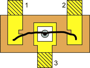
To rapidly fabricate the new configuration, we used low-cost devices in SOT-323 packages from our standard diode portfolio. The PIN diode used has a 1.5 µm I-layer height, ~1 pF zero-bias capacitance, and a dual-anode package style that suits the new configuration (Fig. 2). A thin I-layer was selected for fast response, sensitivity (low limiting threshold), and low spike leakage. The Schottky diode has a 250-mV barrier height (at 1 mA) and a ~0.8-pF zero-bias capacitance. The parasitic inductances associated with the diodes’ bond-wires and leads are 0.7 nH and 0.4 nH, respectively.
 |
|
| Figure 2. | This internal view of the PIN diode shows where the anode contact on the chip is wire-bonded to two connection pins. |
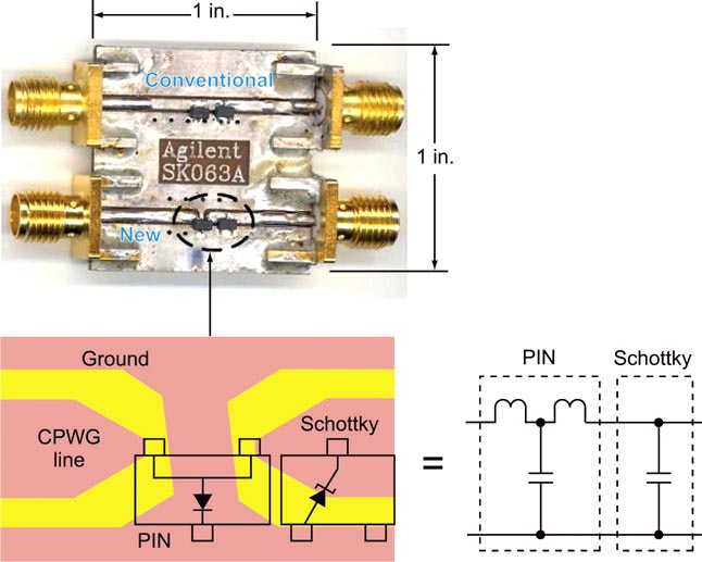
The limiter was built on a 30-mil thick FR-4 printed-circuit board (PCB) with a 50-Ω co-planar waveguide, with grounded coplanar waveguide (CPWG) transmission line having a gap in the middle (Fig. 3). The PIN diode is mounted with its anode leads straddling the gap. The Schottky diode is connected to the output side of the transmission line, as is usually done for this class of limiter. The combination of a dual-anode PIN diode, a Schottky diode, and a gapped line results in a small-signal equivalent circuit that approximates a low-pass ladder filter.
 |
|
| Figure 3. | A PCB with the evaluation and the reference limiters implements the proposed design (top). A close-up diagram (bottom left) and schematic illustration (bottom right) clarify the simplified equivalent circuit of the evaluation limiter. |
For performance comparison, a conventional PIN-Schottky limiter was assembled on a continuous transmission line on the same PCB. Identical diode devices are used in both limiters. Since both diodes are paralleled in the conventional limiter configuration, its small-signal equivalent circuit can be represented by a 1.8-pF capacitor.
Results And Discussion
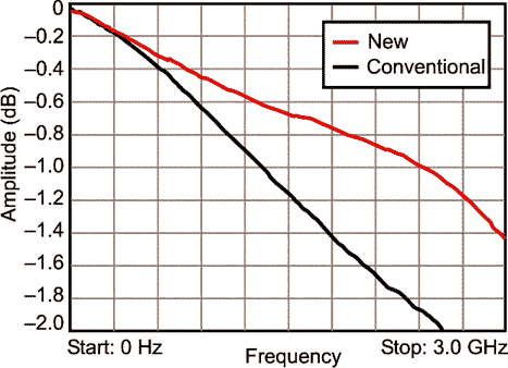
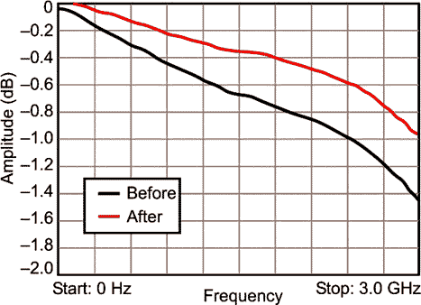
The experimental results confirm that the new configuration improves the insertion loss and the bandwidth performance. Both configurations have almost similar insertion losses below 300 MHz because the parasitic capacitances have minimal effect at these frequencies. Once the frequency increases past 300 MHz, the loss difference between limiters becomes progressively larger (Fig. 4). The measured loss reduction was an impressive 0.8 dB, measured at the popular 3G frequency of 2.1 GHz. The improvement can also be quantified as a bandwidth increase, as the new configuration nearly doubles the upper-frequency limit from the original 1.3 to 2.4 GHz when compared at the 1-dB loss points.
 |
 |
||
| Figure 4. | There is significant improvement in small-signal insertion loss versus frequency for the new limiter configuration, compared to the conventional design. | Figure 5. | The small-signal insertion loss of the new limiter configuration, measured before and after fixture losses compensation, clearly shows the effect of compensating for fixture losses. |
Real-world results will likely be better than what these measurements suggest, because the test fixture exaggerates the loss. Actual applications are likely to have much shorter PCB traces, and the limiter output will be directly connected to the LNA without an RF connector. When fixture losses are removed by normalization, the limiter’s 1-dB bandwidth soars to 3 GHz (Fig. 5).
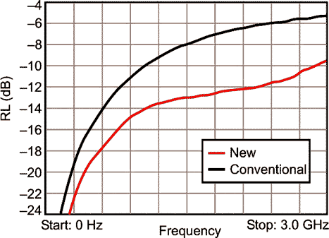
Apart from reducing insertion loss, the new configuration also unexpectedly improves the return loss (RL), particularly in the 1.2- to 3-GHz range where the change exceeds 4 dB (Fig. 6). Apparently, the new configuration’s ladder-filter equivalent circuit presents a better match than the original’s shunt capacitor. The new configuration nearly triples the upper-frequency limit to 2.9 GHz compared to the conventional configuration’s 1.1-GHz value, for the point where RL stays below –10 dB.
 |
 |
||
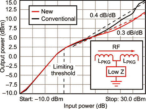
| Figure 6. | The return loss versus frequency of the conventional and new limiter configurations indicates improvement between 4 and 6 dB over most of the range. | Figure 7. | The output versus input power of the conventional and new configurations at 900.1 MHz demonstrate how the PIN diode’s package inductances aid isolation when the diode is in a low-resistance state. |
The ladder network does not change the limiting threshold, but the maximum isolation is improved. Both configurations have similar ~3-dBm input-limiting threshold at 900 MHz (Fig. 7). As an unforeseen benefit, the new configuration’s output-leakage power, at 30-dBm input power, is about 4 dB lower. In the new configuration, the package inductances (LPKG) aid isolation because they are in series with the signal path, whereas they are shunting the signal path in the original configuration. The plateau region is also flatter (0.3 dB/dB) in the new configuration.
 |
|
 |
|
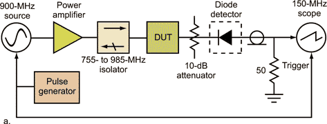
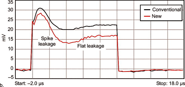
| Figure 8. | In the block diagram of the test setup used to evaluate the transient responses of both limiter configurations (a), note the spike-leakage and flat-leakage amplitudes are about 5 mV lower for the new configuration (b). |
The ladder network does not slow the limiter’s transient response. Furthermore, it reduces the initial spike energy. The limiters’ transient response was measured using a stimulus consisting of a 10-µs burst of 30 dBm/900 MHz carrier [P(W) × t(s) = 10-6J]. The spike-leakage durations are approximately equal (~2 μs) for both configurations (Fig. 8). However, the spike energy, as represented by the area under the graph, is beneficially lower in the new configuration. Both spike-leakage and flat-leakage amplitudes are also lower in the new configuration.
 |
|
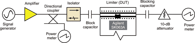
| Figure 9. | The test setup used for measuring the limiter's input-output power relationship must minimize measurement artefacts. The attenuator helps avoid power-sensor burnout. |
Note that at the upper range of the swept-power measurement, the saturated limiter diodes approximate a short across the transmission line. The isolator and the attenuator in the test setup of Figure 9 are needed to eliminate measurement artefacts that appear as a dip in the graph of Figure 7. At the output of the device under test (DUT), a 10-dB attenuator is a better choice than an isolator because, aside from buffering the DUT's impedance change, it can prevent power sensor burn-out.
Conclusion
This new circuit arrangement for the Schottky-PIN limiter simultaneously improves insertion loss, matching, bandwidth, and leakage power, compared the original configuration. The change requires neither additional components nor a bigger PCB area, because it opportunistically uses the diode packages’ inherent parasitics to form a low-pass ladder filter.
Although these parasitics already have been successfully manipulated into a low-pass network to reduce loss in a PIN diode-only limiter, the results show that similar benefits can be obtained in the Schottky-enhanced PIN limiters. The new configuration will improve sensitivity performance in wireless communication and NMR/MRI receivers that use this class of limiter. It should also enable limiter diodes in plastic packages to be used at higher frequencies.