Analog Dialogue
Instrumentation amplifiers (in-amps) can condition the electrical signals generated by sensors, allowing them to be digitized, stored, or used to control processes. The signal is typically small, so the amplifier may need to be operated at high gain. In addition, the signal may sit on top of a large common-mode voltage, or it may be embedded in a substantial DC offset. Precision in-amps can provide high gain, selectively amplifying the difference between the two input voltages while rejecting signals common to both inputs.
 |
|
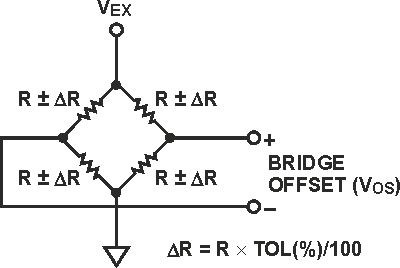
| Figure 1. | Wheatstone bridge offset. |
Wheatstone bridges are classic examples of this situation, but galvanic cells such as biosensors have similar characteristics. The bridge output signal is differential, so an in-amp is the preferred device for high-precision measurements. Ideally, the unloaded bridge output is zero, but this is true only when all four resistors are exactly equal. Consider a bridge built with discrete resistors, as shown in Figure 1. The worst case differential offset, VOS, is
 |
(1) |
where VEX is the bridge excitation voltage and TOL is the resistor tolerance (in percent).
For example, with 0.1% tolerance for each one of the individual elements and a 5-V excitation voltage, the differential offset can be as high as 5 mV. If a gain of 400 is required to achieve the desired bridge sensitivity, the offset becomes ±2 V at the amplifier output. Assuming that the amplifier is powered by the same supply, and that its output can swing rail-to-rail, more than 80% of the output swing could be consumed by the bridge offset alone. As the industry trends to smaller supply voltages, this problem only gets worse.
 |
|
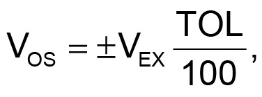
| Figure 2. | 3-op-amp instrumentation amplifier topology. |
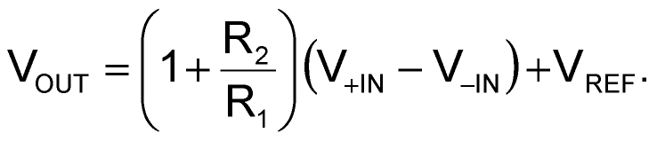
The traditional 3-op-amp in-amp architecture, shown in Figure 2, has a differential gain stage followed by a subtractor that removes the common-mode voltage. The gain is applied on the first stage, so the offset is amplified by the same factor as the signal of interest. Thus, the only way to remove it is to apply the opposite voltage to the reference (REF) terminal. The main limitation of this method is that adjusting the voltage on REF cannot correct the offset if the first stage of the amplifier is already saturated. A few approaches to get around this limitation include:
- Shunting the bridge with an external resistor on a case-by-case basis, but this is impractical for automated production and does not allow for adjustments after leaving the factory
- Reducing the first-stage gain, removing the offset by trimming the voltage on REF, and adding a second amplifier circuit to achieve the desired gain
- Reducing the first-stage gain, digitizing the output with a high-resolution ADC, and removing the offset in software
The two last options also need to account for worst-case deviations from the original offset value, further reducing the maximum gain of the first stage. These solutions are not ideal, as they require extra power, board space, or cost to obtain the high first-stage gain needed to obtain high CMRR and low noise. In addition, ac coupling is not an option for measuring dc or very slow-moving signals.
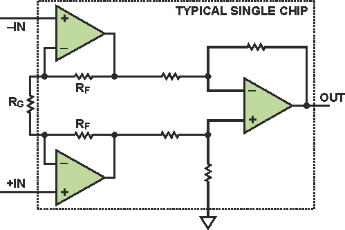
Indirect current feedback (ICF) in-amps, such as the AD8237 and AD8420, make it possible to remove the offset before it is amplified. Figure 3 shows a schematic of the ICF topology.
 |
|
| Figure 3. | Indirect current feedback in-amp topology. |
The transfer function for this instrumentation amplifier is of the same form as that of the classical 3-op-amp topology, and is given by
 |
(2) |
Because the feedback to the amplifier is satisfied when the voltage between the inputs is equal to the voltage between the feedback (FB) and reference (REF) terminals, we can rewrite this as
 |
(3) |
This suggests that introducing a voltage equal to the offset across the feedback and reference terminals allows the output to be adjusted to zero volts even in the presence of a large input offset. As shown in Figure 4, this adjustment can be accomplished by injecting a small current into the feedback node through resistor RA from a simple voltage source such as a low-cost DAC or a filtered PWM signal from an embedded microcontroller.
Design Procedure
From Equation (3), the ratio of R1 and R2 sets the gain as follows:
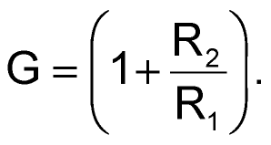 |
(4) |
The designer must determine the resistor values. Larger values reduce power consumption and output loading; smaller values limit the input bias current at FB and input impedance errors. If the parallel combination of R1 and R2 is greater than about 30 kΩ, the resistors start to contribute to the noise. Table 1 shows some suggested values.
| Table 1. | Suggested Resistors for Various Gains (1% Resistors) |
|||||||||||||||||||||||||||||||||
|
||||||||||||||||||||||||||||||||||
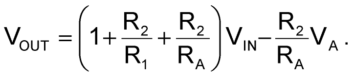
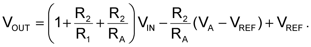
To simplify the process of finding a value for RA, assume dual- supply operation, a grounded REF terminal, and a known bipolar adjustment voltage VA. In this case, the output voltage is given by
 |
(5) |
Notice that the gain from VA to the output is inverting. An increase in VA reduces the output voltage by a fraction given by the ratio of resistors R2 and RA. This ratio allows the adjustment range to be maximized for a given input offset. Because the adjustment range is referred to the input of the amplifier before gain, fine adjustment steps can be achieved even with a low resolution source. Since RA is typically much larger than R1, we can approximate Equation (5) as
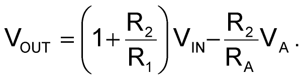 |
(6) |
To find a value of RA that will allow a maximum offset adjustment, VIN(MAX), with a given adjustment voltage range, VA(MAX), set VOUT = 0 and solve for RA, giving
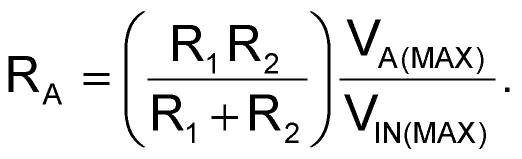 |
(7) |
where VIN(MAX) is the maximum offset expected from the sensor. Equation (5) also shows that the insertion of the adjustment circuit modifies the gain from the input to the output. Even though this will generally have a small effect, the gain can be recalculated as
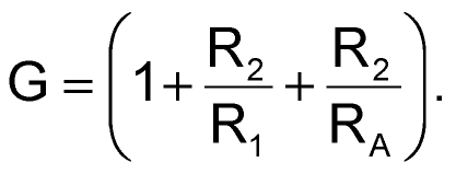 |
(8) |
In general, for single-supply bridge conditioning applications, the voltage on the reference terminal should be above the signal ground. This is especially true if the bridge output can swing positive and negative. If the reference voltage is driven to a voltage, VREF, with a low-impedance source such as a resistor divider and a buffer, as shown in Figure 5, Equation (5) becomes
 |
(9) |
This same result would be obtained if VOUT and VA were taken relative to VREF in the original equations. VA(MAX) – VREF should also replace VA(MAX) in Equation (7).
Design Example
Consider a single-supply bridge amplifier such as that shown in Figure 4, where 3.3 V is used to excite the bridge and power the amplifier. The full-scale bridge output is ±15 mV, and the offset can be in the ±25-mV range. To obtain the desired sensitivity, the amplifier gain needs to be 100, and the input range of the ADC is 0 V to 3.3 V. Because the output of the bridge can be positive or negative, the output is referenced to midsupply, or 1.65 V. Simply by applying a gain of 100, the offset alone would force the amplifier output to be anywhere from –0.85 V to +4.15 V, which exceeds the supply rails.
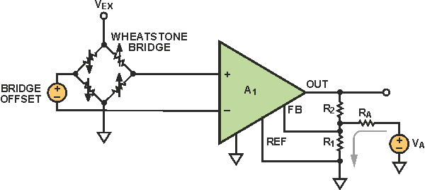 |
|
| Figure 4. | High gain bridge circuit with offset removal. |
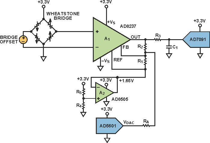
This problem can be solved with the circuit shown in Figure 5. Bridge amplifier A1 is an ICF instrumentation amplifier such as the AD8237. Amplifier A2, with R4 and R5, sets the zero level output of A1 at midsupply. The AD5601 8-bit DAC adjusts the output to null the bridge offset through RA. The output of the amplifier is then digitized by the AD7091 micropower 12-bit ADC.
 |
|
| Figure 5. | Offset removal circuit modified for single-supply operation. |
From Table 1, we find that R1 and R2 need to be 1 kΩ and 100 kΩ for a gain of 101. The circuit includes a DAC that can swing from 0 V to 3.3 V, or ±1.65 V around the 1.65-V reference voltage. To calculate the value of RA we use Equation (6). With VA(MAX) = 1.65 V and VIN(MAX) = 0.025 V, RA = 65.347 kΩ. With 1% resistor tolerance, the closest available value is 64.9 kΩ. This leaves no margin for errors caused by source accuracy and temperature variation, however, so we choose a low cost, commonly stocked 49.9-kΩ resistor. The trade-off is reduced adjustment resolution, which results in a slightly larger post-adjustment offset.
From Equation (7), the nominal gain value can be calculated to be 103. If the designer wants to obtain a gain value closer to the target of 100, it is easiest to reduce the value of R2 by about 3% to 97.6 kΩ, which will have very little influence on the value of RA. Under the new conditions, the nominal gain is 100.6.
Because the DAC can swing ±1.65 V, the total offset adjustment range is given by the voltage divider formed by RA and the parallel combination of R1 and R2, which can be calculated as follows:
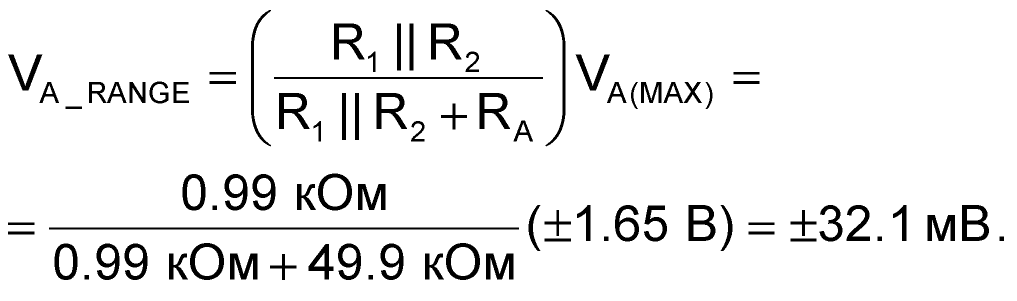 |
(10) |
A ±32.1-mV adjustment over the ±25-mV maximum bridge offset provides an additional 28% adjustment margin. With an 8-bit DAC, the step size for the adjustment is
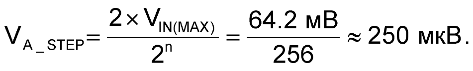 |
(11) |
With a 250-µV adjustment resolution, the maximum residual offset at the output is 12.5 mV.
The values of R3 and C1 can be determined from the values suggested in the ADC data sheet or from Reference 2. For an AD7091 sampling at 1 MSPS, these values are 51 Ω and 4.7 nF. Larger resistor and capacitor combinations can be used when sampling at lower rates to further reduce noise and aliasing effects.
An additional advantage of this circuit is that the bridge offset adjustment can be done at production or installation. If environmental conditions, sensor hysteresis, or long-term drift have an effect on the value of the offset, the circuit can be readjusted.
Because of its true rail-to-rail input, the AD8237 works best in bridge applications that employ very low supply voltages. For traditional industrial applications where higher supply voltages are required, the AD8420 is a good alternative. This ICF in-amp operates with supply voltages from 2.7 V to 36 V and draws 60% less current.
Table 2 compares the two in-amps. Minimum and maximum specifications have been used where available. See the product data sheets for more detailed and up to date information.
| Table 2. | Comparison of AD8237 and AD8420 | |||||||||||||||||||||||||||||||||||||||||||||
|
||||||||||||||||||||||||||||||||||||||||||||||
References
- AN212 Application Note. Handling Sensor Bridge Offset. Honeywell International Inc., Rev 05-05.
- HMC1001/HMC1002/HMC1021/HMC1022 1- and 2-Axis Magnetic Sensors Data Sheet. Honeywell International Inc., 2008.
- Kitchin, Charles and Lew Counts. A Designer’s Guide to Instrumentation Amplifiers. 3rd Edition. Analog Devices, Inc., 2006.
- NPC-410 Series Data Sheet. GE Sensing, 2006.
- Product Training Module. Indirect Current Feedback Instrumentation Amplifier Applications Guide. Digi-Key Corporation.
- Walsh, Alan. “Front-End Amplifier and RC Filter Design for a Precision SAR Analog-to-Digital Converter.” Analog Dialogue, Volume 46, 2012.