Loren Siebert, Texas Instruments
As high-speed systems become more complex and design cycles become shorter, engineers need to find high-performance yet flexible components to facilitate their system designs. One method is to use components that offer very high performance, yet are easy to reconfigure to produce new products, or can be quickly reconfigured to correct issues discovered late in the design cycle. Finding parts that offer both high performance and flexibility is a challenge. Now there is a new class of differential amplifiers to meet the needs of engineers.
This article explains the architectural features of the industry’s first programmable differential amplifier (PDA), including its easy-to-change voltage gain, consistent bandwidth over gain settings, constant input impedance over gain settings, excellent linearity, and low-noise figure. The PDA is compared to the fully differential amplifier (FDA) and digital variable gain amplifier (DVGA). Configuring the PDA’s gain and input configurations are also discussed.
The industry’s first PDA, the LMH6881, is a high-speed, high-performance, fully differential amplifier. With a bandwidth of 2.4 GHz and an OIP3 of 44 dBm, it addresses a wide variety of signal conditioning applications from radio equipment to high-speed test and measurement systems. The PDA combines the best of FDAs and DVGAs. It offers superior noise and distortion performance over the entire gain range without external resistors, enabling the use of one device for many applications requiring different gain settings.
PDA vs. FDA
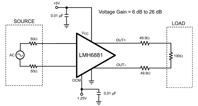
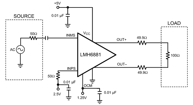
The PDA was designed to make differential amplifier circuits easy to implement. It can be used in place of a traditional fully differential, fixed gain amplifier (Figure 1). Because the gain is easily changed, the PDA supports last minute design changes while accommodating variability in other parts of the signal chain.
 |
|
| Figure 1. | Typical connection of the programmable differential amplifier. |
Traditional FDAs require external components to set the closed-loop gain (Figures 4 and 5). The PDA’s gain can be easily changed by either the external gain set pins or with the internal serial peripheral interface (SPI) register. For fixed gain applications, the external gain set pins can be connected directly to ground or the 5 V supply.
In addition to fixed gain applications, the PDA also supports rapid gain changes. In parallel mode, gain changes require only 20 ns. The PDA requires no external resistors to set the closed-loop gain. Gain can be set in 2 dB increments by external pins, or an internal gain register allows the use of 0.25 dB gain steps. The internal gain register is accessed through an SPI-compatible control bus.
 |
|
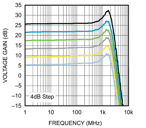
| Figure 2. | PDA frequency response with 4 dB voltage gain steps. |
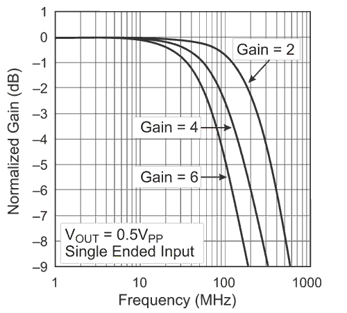
In contrast to a typical FDA, the PDA offers consistent bandwidth performance over a wide voltage gain range. With an FDA, the bandwidth, noise figure and distortion performance all change significantly over the usable gain range. The FDA has large changes in loop gain when the closed-loop gain is altered. As shown in Figure 2, the PDA’s frequency response is insensitive to voltage gain. The frequency response graph of a traditional FDA (Figure 3) shows a frequency response with the well-documented gain bandwidth product.
 |
|
| Figure 3. | Traditional FDA frequency response. |
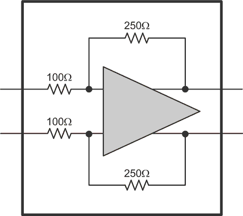
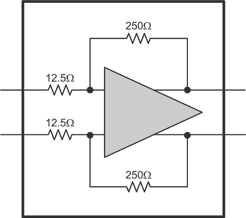
The input is terminated at 100 Ohm for differential signals, and the input termination is independent of gain. In contrast, a FDA has to balance input impedance with realistic gain set resistor values. Two FDA circuits are shown in Figures 4 and 5, with one set at 8 dB of gain and the other at 26 dB. From this example, it’s obvious that the input impedance changes drastically between the two gain settings. In addition to the input impedance, the noise contributed by external resistors is different.
 |
 |
||
| Figure 4. | Traditional FDA with 8 dB gain. | Figure 5. | FDA with 26 dB gain. |
PDA vs. DVGA
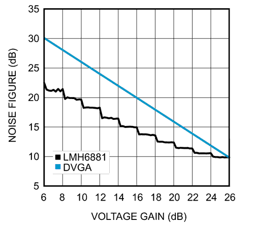
The PDA has an internal architecture that avoids the 1:1 increase in noise figure with gain changes that is characteristic of a traditional DVGA (Figure 6). This allows the PDA to maintain a good dynamic range figure throughout the entire gain range.
 |
|
| Figure 6. | PDA noise figure compared to traditional DVGA noise figure. |
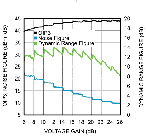
Figure 7 shows the PDA’s OIP3 is consistent across the entire voltage gain range. Moreover, its noise figure is more consistent than with most variable gain amplifiers. The noise figure changes only 12 dB across a 20 dB gain range.
 |
|
| Figure 7. | Dynamic range figure uses OIP3, NF to characterize input dynamic range capabilities. |
Figure of merit calculation
The value of the PDA’s performance is captured by a figure of merit called the dynamic range figure. This figure of merit is calculated by subtracting the noise figure (NF) from the input third-order intercept point (OIP3). The dynamic range figure is a good proxy for the overall dynamic range of an amplifier. With a traditional DVGA, the figure of merit is highest at maximum gain and decreases rapidly as the noise figure increases with lower gain settings. With a PDA, the maximum value of the dynamic range figure is in the middle of the gain range with only gradual changes realized as the voltage gain is changed.
 |
 |
||
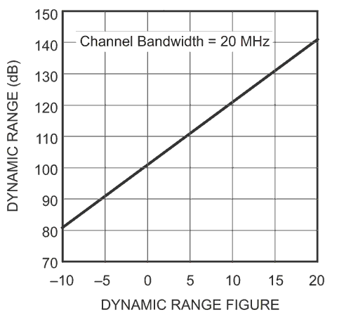
| Figure 8a. | Dynamic range vs. Dynamic Range Figure. | Figure 8b. | This graphic illustrates dynamic range for an amplifier. |
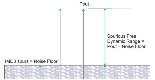
The chart in Figure 8a shows the relationship between the dynamic range figure and the maximum available dynamic range at the input of the amplifier. In this example, the channel bandwidth is 20 MHz and the overall dynamic range is the difference between the peak amplitude of the two intermodulation tones and the noise floor. The spurious free dynamic range (or dynamic range) is at a maximum when the power of the IMD3 spurs is equal to the noise floor. This is illustrated in Figure 8b. If the output power is increased, the IMD3 spurs increase at three times the rate of the increase in output power. If the output power decreases, the noise floor will not change – even though the IMD3 spurs fall in amplitude.
PDA input configurations
The PDA can accept a fully differential input signal on the two differential input pins (Figure 9). The input impedance is set by an on-chip resistor to 100 Ohms. By having a fixed input impedance, the PDA does not need external resistors to match many common signal sources. If a higher input impedance is desired, external resistors can be used. The PDA also has the option of accepting a single-ended input.
 |
|
| Figure 9. | Input configuration for single-ended signal. |
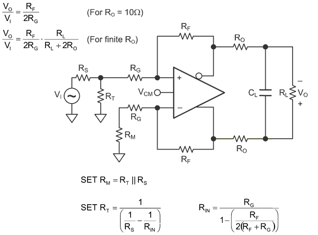
By using the single-ended input pins, the PDA can be configured to accept 50 Ohm signals. In this case, only one 50 Ohm external resistor is required. In contrast, the schematic (Figure 10) shows what is required to set the input impedance for a traditional FDA when using a single-ended signal source. What makes things even more complicated is that a change in the FDA’s gain requires a change in resistors. With the new PDA architecture, the input impedance is fixed at a convenient 50 Ohms and does not change as the voltage gain changes.
 |
|
| Figure 10. | Traditional FDA input impedance calculations. |
The PDA offers many benefits including constant bandwidth, fixed input impedance, excellent linearity and good noise figure. These attributes make PDAs easy to use in complex systems or in systems that may require last minute design changes.
 |
|
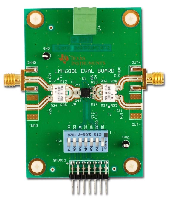
| Figure 11. | LMH6881 PDA evaluation board. |
An evaluation board (Figure 11) enables engineers to immediately begin PDA testing and system development. To make the board easy to use, transformers are provided to convert the differential signals at the PDA’s input and output into single 50 Ohm signals. Gain can be set with the blue DIP switch, or it can be changed using the 0.1 inch header.
Conclusion
Designing with high speed operational amplifiers (op amps) can be challenging. Simultaneously achieving high levels of performance across multiple specification requirements such as bandwidth, noise, distortion and impedance can be tricky. Most designers can vouch for how tedious it can be to redesign and optimize the signal chain for a different gain value. The new PDA class of differential amplifier enables flexible and effortless signal chain design, allowing engineers to use one chip and one design for a broad range of applications.