Bruce Archambeault
EDN
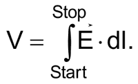
 A friend of mine told me years ago that there's no such thing as voltage. This was a real shock to me, because I had a voltmeter in the lab. He explained that Maxwell's equations, which are accepted as the basis for all electromagnetic (and therefore circuit) theory, include current, electric field, and magnetic field, but no voltage. In fact, "voltage" is a derived term shown in the equation below. It is the summation (integration) of the electric field over a distance:
Most PCB designers talk about things such as DC supply voltage or a signal voltage on traces. If I bring up the idea of current flow, they will accept it. Then we discuss how the return current always flows back to its source on ground.
The term "ground" is probably the most misunderstood and misused term in electrical engineering. I blame the universities. They start their electrical engineering instruction with DC circuits and then progress to AC circuits with resistors, inductors, and capacitors. But the ideas of parasitic and nonschematic effects are seldom discussed in classes. Usually, lab assignments are relatively low-frequency projects, probably designed to ensure parasitic effects aren't encountered.
We learn to read schematics with this magical return current path called ground. At low frequencies, the physical distance between the ground connections is electrically small. This concept of having all ground nodes connected at the same point is reasonable.
In the real world of high-speed circuit boards, the physical distance between ground node connections isn't electrically small, so the distance between the nodes becomes meaningful. Current must travel some distance to return to its starting point. This distance can adds losses that make ground something else entirely.
For example, let's take a microstrip trace over a metal plane, but let's have a PCB stack up where the metal plane is assigned as 3.3 V (not "ground"). A ground plane will exist lower in the PCB stack. The schematic will indicate the return current path is ground, not 3.3 V. Unfortunately, the current does not read the schematic to see where the designer intended the current to flow. It will follow the path of least impedance. At frequencies higher than about 1 MHz, this means the path of least inductance. That path will nearly always have the smallest current loop size, so the current will flow on the 3.3 V plane, not the ground plane.
The image below shows the electric field lines for a microstrip. Where those field lines terminate, current will flow (into or out of the page). Even though the signal on the trace was driven relative to a ground plane (which is not shown) below the VCC plane, the field lines terminate on the VCC plane. The return current will always flow in the nearest plane, regardless of its schematic name.
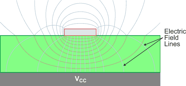 |
| Electric field lines for a microstrip. (Source: Hyperlynx) |
How does the return current get on a conductor that is not called for in the schematic? After all, we solder the ground pin on the IC to the ground plane, not the VCC plane. The image below shows that, even though the current driven down the signal trace goes into the capacitive load of the CMOS IC at the load end and to the ground pin, it migrates to the VCC conductor once the return current gets a little distance from the IC.
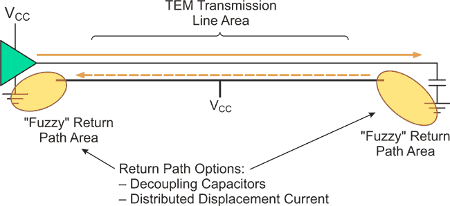 |
| Zero-to-one transition current path for CMOS devices. |
The actual migration path (or fuzzy return path) depends on the location of decoupling capacitors, the displacement current through the PCB dielectric, etc. The exact path will differ for each case, and it would require full wave analysis to predict the path accurately.
I am fond of saying ground is a place for potatoes and carrots. When working with moderate- or high-speed PCBs, the concept of ground is unimportant. The return current path is the most important issue. Engineers always take great care to make sure the intentional signal path is connected as desired, but they seldom consider the return current path. Interruptions in the return current path are the most common cause of PCB-related EMC issues, both for immunity and for emissions. Many signal integrity issues can also be traced to poorly designed return current paths.
 |
| Ground is a place for potatoes and carrots. |