Maria Guerra
Electronic Design
Dr. James R. “Bob” Biard (born May 20, 1931) is an American electrical engineer and inventor who holds 72 U.S. patents, including the GaAs infrared light-emitting diode (LED), the optical isolator, the Schottky transistor, and Metal Oxide Semiconductor Read Only Memory (MOS ROM). He has been on the staff of Texas A&M University as an Adjunct Professor of Electrical Engineering since 1980. This year marks 55 years since Dr. Biard and Gary Pittman first observed light emission from a GaAs LED at Texas Instruments (TI) in Dallas. Recently he spoke with Technology Editor Maria Guerra, sharing his memories and thoughts on a number of topics.
Your biography mentions your employment at TI began in 1957, three days after you received your PhD from Texas A&M. This was one year prior to the hiring of Jack Kilby, the inventor of the integrated circuit. Do you recall what the atmosphere was like at the TI plant in the summer of 1958 when he developed his first germanium IC?
 |
||
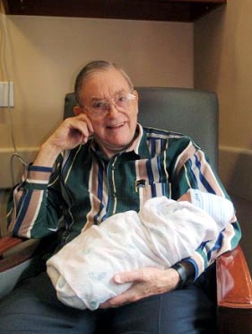
| Retirement suits Texas Instruments' legend James "Bob" Biard just fine. |
||
It was a very exciting time. A lot of interesting things were happening. Transistors up until Kilby’s time had been mainly grown junction, alloy junction, or mesa devices made from either germanium or silicon. All these were discrete transistor chips mounted in headers of various kinds, which had three leads (emitter, base, and collector). These transistors were used with other components like resistors and capacitors for constructing useful electronic circuits normally on printed circuit boards. This gave a dramatic size reduction compared to earlier vacuum tube versions of similar circuits. However, as the circuits became more complex, the transistor circuits also became quite large.
Since Kilby had been recently hired, he had no vacation time. He worked while everyone else took mass vacation, which was the practice at TI at that time. During that mass vacation he came up with a unique insight into a technique that would dramatically reduce the size of electronic circuits by making the transistors, resistors, and capacitors all from the semiconductor. His first integrated circuit was a single stage amplifier made from germanium. It included a transistor, resistors, and a P-N junction diode used as a capacitor all made in the same germanium chip. These circuit elements were interconnected by wire bonds. Based on his insight, TI filed a patent for the integrated circuit. However, the germanium integrated circuit never caught on as a product. The semiconductor industry was just beginning to develop silicon planar technology and about six months later Robert Noyce at Fairchild Semiconductor came up with a technique for interconnecting transistors, resistors, and P-N junction capacitors into a working circuit using aluminum metallization over a silicon dioxide layer formed on the surface of the planar silicon chip. This was the development that made Kilby’s original idea for the integrated circuit practical. Kilby and Noyce are often thought of as the co-inventors of the integrated circuit. Kilby’s basic idea came first, but Noyce made it work. Robert Noyce died in 1990 at age 62. Kilby received the Nobel Prize in Physics for the invention of the integrated circuit in 2000 and died in 2005 at age 81.
Jack Kilby was my boss for several years prior to 1969 when I worked for TI and he was instrumental in getting me started as a part-time Adjunct Professor of Electrical Engineering at Texas A&M.
One of your first projects at TI was working on a low drift dc amplifier with your former Texas A&M professor, Walter T. Matzen. This work ultimately led to one of your first patents, the DC differential amplifier. Can you mention a few details about how this patent came about and its significance?
Walter Matzen was my major professor at A&M and he also served on my graduate committee. We both went to work at TI on June 3, 1957, and continued to work together for some time. My education in semiconductors began with my employment at TI. The main emphasis of our first project was on describing the characteristics of the bipolar transistor that affect offset and drift. There are two main parameters: 1) The way the emitter-base voltage depends on collector current and temperature, and 2) The dependence of the base current on collector current and temperature. After describing these dependencies, we went on to develop a low offset transistorized dc differential amplifier with low drift over temperature. The amplifier was implemented using carefully matched pairs of discrete grown junction silicon transistors.
We filed our patent in March of 1958. We then published an article in Electronics magazine in January of 1959. Honestly, I don't remember if our transistor dc amplifier was the first or just one of the first. Things were happening pretty fast back then. However, the drift equivalent circuit and method of analysis developed on this program formed the basis for much of the work that followed at TI on differential transistor amplifiers. With one of the electronics technicians, we designed and constructed one of the first completely automatic transistor testing facilities. It was called the Sequential Mechanism for Automatic Recording and Testing (SMART). SMART-1 could perform up to 18 ac and dc tests on a transistor and record the results of these tests directly on an IBM card without human intervention. This work resulted in a commercial line of SMART machines, which were manufactured and sold by the Industrial Instrumentation Division at TI. The commercial SMART machines were used primarily for incoming lot acceptance and life testing where it was necessary to maintain unit identification with recorded values of measured parameters.
 |
||
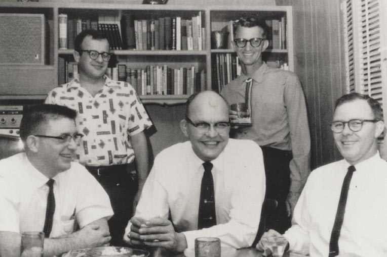
| Texas Instruments engineers in Dallas in the early 1960s. From left to right: Standing, Charles Phipps, Joe Weaver; Seated, James R. Biard, Jack Kilby, and James Fischer. |
||
In September 1961, you and your LED co-inventor Gary Pittman were working on a project to develop GaAs varactor diodes when you first observed light emission. Can you explain what you two were investigating when you built the test structure on the GaAs substrate?
We initially thought we were seeing excess current in the valley region of the tunnel diodes we were building and felt this could have an impact on the varactor diodes. I came up with a theory to describe the excess current as a radiative recombination generation in which an emitted photon was stimulating other centers to discharge. Based on this theory, I thought it might be possible to use the stimulated emission to make a GaAs laser diode. We built the structure with the tunnel diode on a semi-insulating GaAs substrate to test the theory and found that the excess current was actually occurring in the forward bias region of the diode curve. When we forward biased the tunnel diode, it changed the conductivity of the semi-insulating GaAs substrate. This made us think that the GaAs diodes might be emitting photons. However, the light being emitted was infrared, which is not visible to the human eye. About that time a Japanese firm brought an infrared microscope to TI for the Quality Control Department to use for inspecting silicon wafers. When Gary and I found out it was in the building, we took some GaAs varactor diodes and tunnel diodes with clip leads and batteries to the Quality Control Department. We found that when the varactor and tunnel diodes were forward biased, they all emitted infrared light that could be seen on the infrared microscope. We filed our patent about a year later. The Central Research group at TI was of the opinion that semiconductors did not emit light, but we proved them wrong.
In October 1962, TI released the SNX-100 GaAs LED based on your design. This was the first commercial LED product. In October 1963, TI released the first hemispherical LED product, the SNX-110 GaAs LED. What were the reasons you and your team switched from a flat square crystal to a dome-shaped one?
When the LED chip is rectangular, only about 4% of the internally emitted light is at a small enough angle to escape the top flat surface of the chip. This is because the index of refraction of GaAs is so high (about 3.6), which gives an angle for total internal reflection of about 16.1°. If you could get all of the upward directed light out without absorption, it would increase the output by a factor of 25. When the chip shape is a hemispherical dome with the junction area limited to the central portion of the flat face of the dome, all of the unabsorbed photons emitted at the junction strike the exit surface of the dome at an angle less than the critical angle. That happens when the radius of the dome is greater than the radius of the junction by a ratio equal to or greater than the index of refraction of the GaAs. This increases the light output by a significant amount by eliminating total internal reflection, however, the increase is not by a factor of 25 due to the absorption that happens in the GaAs in the larger radius of the dome. The N-type GaAs between the junction and the exit surface is not completely transparent to the wavelength emitted at the PN junction. The greater path length for the photons in the dome LED structure produces more absorption than the short path length in the rectangular LED chip. However, the hemispherical dome LED resulted in a significant increase in total power output for a given forward bias current compared to the rectangular LED.
In the 1960s, one of the main contributors to integrated circuit research was the U.S. Air Force. Was it a similar situation for the LED?
Yes. Some of the development work we did on LEDs was funded by the U.S. Air Force at Wright Patterson AFB.
In December 1962, Nick Holonyak, Jr., of General Electric reported visible red light emission from an LED. Have you ever met him? If so, did you discuss with him your own work on the LED?
I know Nick Holonyak and have corresponded with him over the years. Apparently my engineering notebook entry for the GaAs tunnel diode on the semi-insulating substrate preceded his group’s earliest work at GE on visible red LEDs in gallium-arsenide-phosphide (GaAsP). When we heard about the work they were doing, we immediately started a program at TI on red LEDs. I once sent Nick a copy of my PowerPoint file that documents the invention of the LED. I think he generally accepts that my IR LED patent preceded his red LED.
Did you know Albert Einstein’s grandson, Bernhard Caesar Einstein, when he worked at TI in the 1960s?
Not that I remember; however, I’ve read we had the same boss, Dr. Richard Petritz. When Gary Pittman and I were in SRDL (Semiconductor Research and Development Laboratory), Dr. Petritz was the director. He supervised over 300 technical personnel. I think Dr. Petritz was in TI’s Central Research division before he transferred over to the Semiconductor Division to head up the SRDL. If Bernhard worked in the Central Research division, that might explain why I didn’t know him. Apparently he worked with Hans Jurg Stocker. I do remember that name. Stocker worked on infrared detectors and indium-antimonide (InSb) diodes. At the time, Gary and I worked almost exclusively on gallium-arsenide and gallium-arsenide-phosphide.