By Aldrick S. Limjoco, Analog Devices
Analog Dialogue
Introduction
Minimizing output ripple and transients from a switching regulator can be important, especially when powering noise-sensitive devices such as high-resolution ADCs, where the output ripple can appear as a distinct spur on the ADC’s output spectrum. To avoid degrading the signal-to-noise ratio (SNR) and spurious-free dynamic range (SFDR), the switching regulator is often replaced with a low-dropout regulator (LDO), trading the high efficiency of the switching regulator for the cleaner output of the LDO. Understanding these artifacts will allow designers to successfully integrate switching regulators in a wider range of high-performance, noise-sensitive applications.
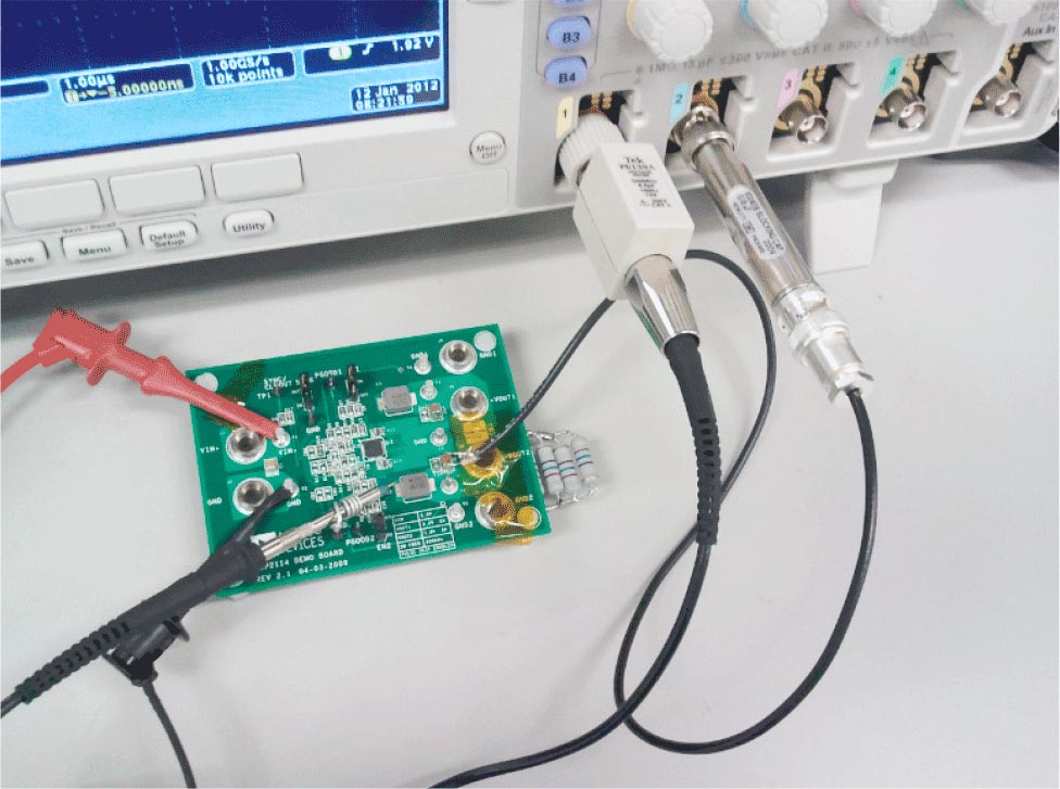
This article describes effective techniques for measuring output ripple and switching transients in switching regulators. Measuring these artifacts requires great care, as a poor setup can lead to incorrect readings, with the loops formed by the oscilloscope probe’s signal and ground leads introducing parasitic inductance. This increases the amplitude of the transients associated with fast switching transitions, so short connections, good techniques, and wide bandwidth must be maintained. Here, the ADP2114 dual 2-A/single 4-A synchronous step-down dc-to-dc converter is used to demonstrate techniques for measuring output ripple and switching noise. This buck regulator provides high efficiency and operates at switching frequencies up to 2 MHz.
Output Ripple and Switching Transients
Output ripple and switching transients depend on the regulator’s topology, as well as the values and characteristics of the external components. Output ripple is a residual ac output voltage that is coherently related to the switching operation of the regulator. Its fundamental frequency is the same as the regulator’s switching frequency. Switching transients are high-frequency oscillations that occur during switching transitions. Their amplitude, expressed as a maximum peak-to-peak voltage, is difficult to measure accurately since it is highly dependent on the test setup. Figure 1 shows an example of output ripple and switching transients.
 |
||
| Figure 1. | Output ripple and switching transients. | |
Output Ripple Considerations
The regulator’s inductor and output capacitor are the main components that affect output ripple. A small inductor gives faster transient response at the expense of higher current ripple, while a large inductor leads to lower current ripple at the expense of slower transient response. Using a capacitor with low effective series resistance (ESR) minimizes the output ripple. A ceramic capacitor with X5R or X7R dielectric is a good choice. A large capacitance is often used to lower the output ripple, but the size and number of output capacitors comes at the expense of cost and PCB area.
Frequency Domain Measurement
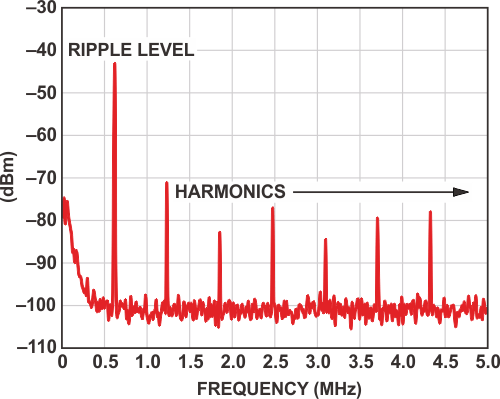
When measuring unwanted output signal artifacts, it is useful for power engineers to think of the frequency domain, as this provides a better perspective as to which discrete frequencies the output ripple and its harmonics occupy with each corresponding power level. Figure 2 shows an example spectrum. This type of information helps engineers to determine whether the chosen switching regulator is appropriate for their wideband RF or high-speed converter applications.
 |
||
| Figure 2. | Frequency domain plot using spectrum analyzer. | |
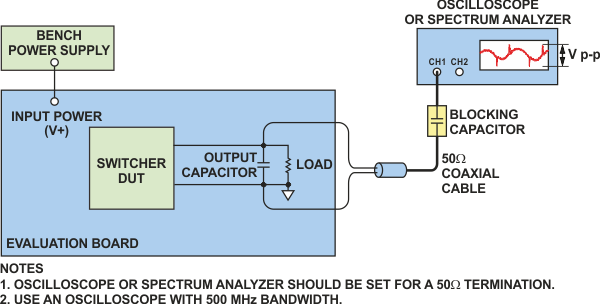
To make a frequency domain measurement, connect a 50-Ω coaxial cable probe across the output capacitor. The signal goes through a dc-blocking capacitor and ends with a 50-Ω termination at the input of the spectrum analyzer. The dc-blocking capacitor prevents dc from passing to the spectrum analyzer and avoids dc-loading effects. The 50-Ω transmission environment minimizes high-frequency reflections and standing waves.
The output capacitor is the main source of output ripple, so the measurement point should be as close as possible. The loop from signal tip to ground should be kept as small as possible to minimize additional inductance that may affect the measurement. Figure 2 shows output ripple and harmonics in the frequency domain. The ADP2114 generates 4-mV p-p output ripple at the fundamental frequency under the specified operating conditions.
Time Domain Measurement
When using an oscilloscope probe, avoid ground loops by eliminating long ground leads, as loops formed by the signal tip and long ground leads create additional inductance and higher switching transients.
 |
||
| Figure 3. | Ground loop causes output errors. | |
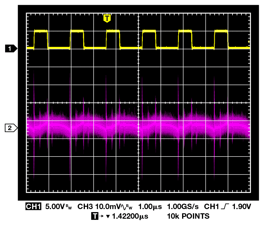
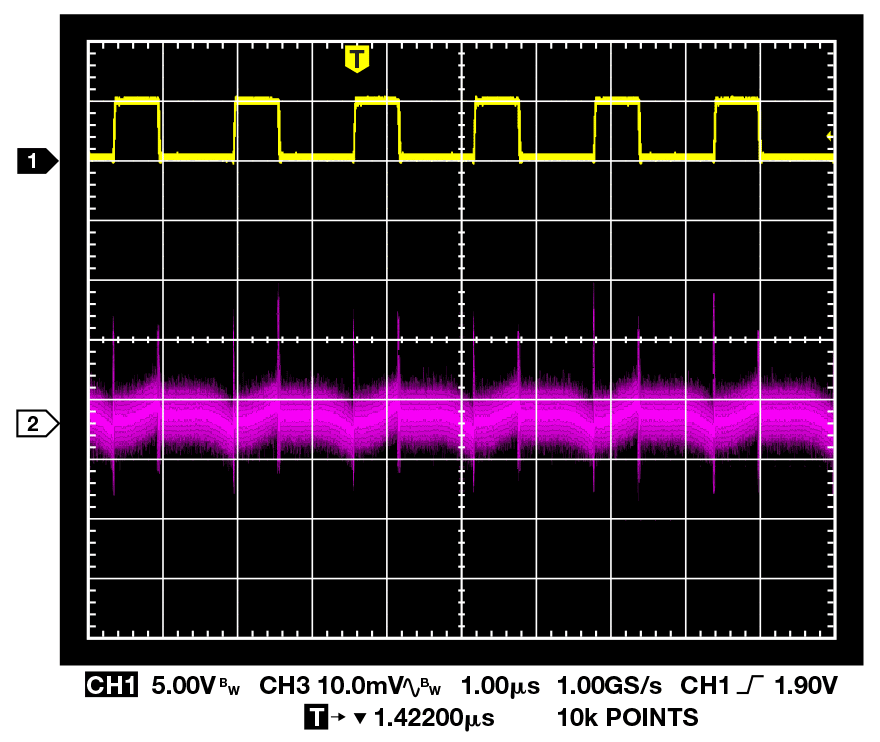
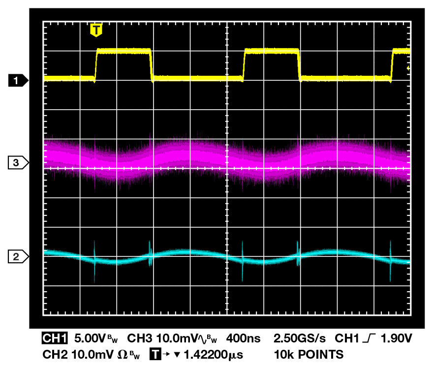
When measuring low-level output ripple, use a 1× passive probe or a 50-Ω coaxial cable rather than a 10× oscilloscope probe, as the 10× probe attenuates the signal by a factor of 10, pushing the low-level signal down towards the scope noise floor. Figure 3 shows a suboptimal probing method. Figure 4 shows the resulting waveform measured using a 500-MHz bandwidth setting. The high-frequency noise and transients are measurement artifacts due to the loop formed by the long ground lead, and are not inherent to the switching regulator.
 |
||
| Figure 4. | Switch node (1) and ac-coupled output waveform (2). | |
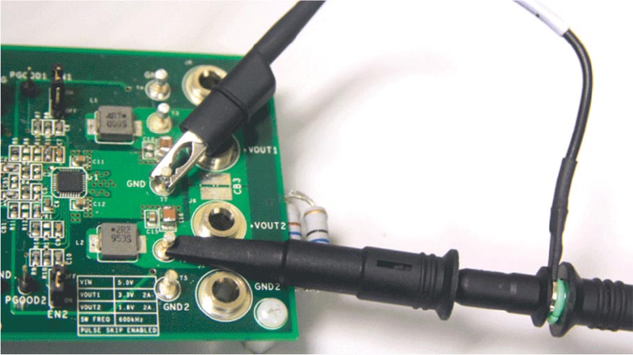
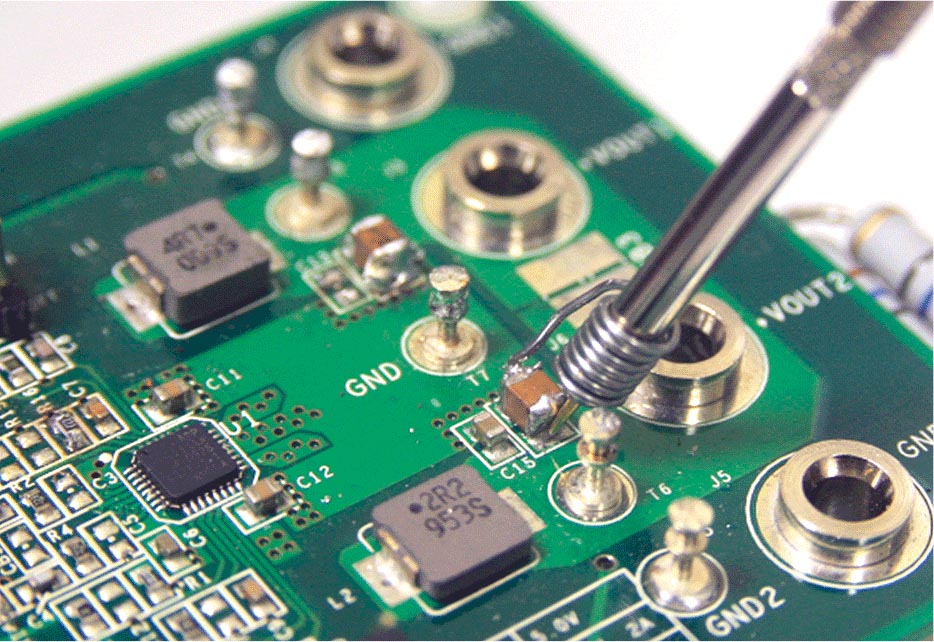
There are a few ways to reduce the stray inductance. One method is to remove the long ground lead from the standard oscilloscope probe, instead connecting the probe’s barrel body to the ground reference. Figure 5 shows the tip-and-barrel method. In this case, however, the tip is connected at the wrong point of the regulator output, rather than directly on the output capacitor as it should be. The ground lead was removed, but the inductance caused by the trace on the PC board remains. Figure 6 shows the resulting waveform using a 500-MHz bandwidth setting. The high-frequency noise is smaller because the long ground lead was removed.
 |
||
| Figure 5. | Tip-and-barrel method probed on random point of switcher’s output. | |
 |
||
| Figure 6. | Switch node (1) and ac-coupled output waveform (2). | |
 |
||
| Figure 7. | Tip-and-barrel method probed on output capacitor using coil wire ground. |
|
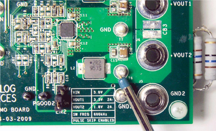
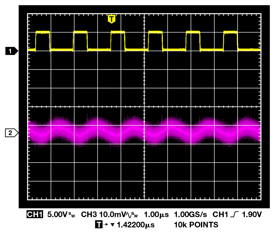
As shown in Figure 7, probing directly on the output capacitor using a grounded coil wire produces nearly optimal detail in the output ripple. Noise at the switching transition is improved, and trace inductance on the PCB is significantly reduced. However, a low-amplitude signal silhouette is still superimposed on the ripple, as shown in Figure 8.
 |
||
| Figure 8. | Switch node (1) and ac-coupled output waveform (2). | |
Best Method
 |
||
| Figure 9. | Best probing method uses an end-terminated 50-Ω coaxial cable. | |
 |
||
| Figure 10. | Example of best probing method. | |
The best method for probing the switcher’s output uses a 50-Ω coaxial cable maintained in a 50-Ω environment and terminated by the oscilloscope’s selectable 50-Ω input impedance. A capacitor placed between the regulator’s output capacitor and the oscilloscope’s input blocks dc flow. The other end of the cable can be soldered directly to the output capacitor using very short flying leads, as shown in Figure 9 and Figure 10. This preserves signal integrity when measuring very low-level signals over a wide bandwidth. Figure 11 shows a comparison of the tip-and-barrel method and the 50-Ω coaxial method probed on the output capacitor using a 500-MHz measurement bandwidth.
 |
||
| Figure 11. | Switch node (1), tip-and-barrel method (3), and 50-Ω coaxial method (2). |
|
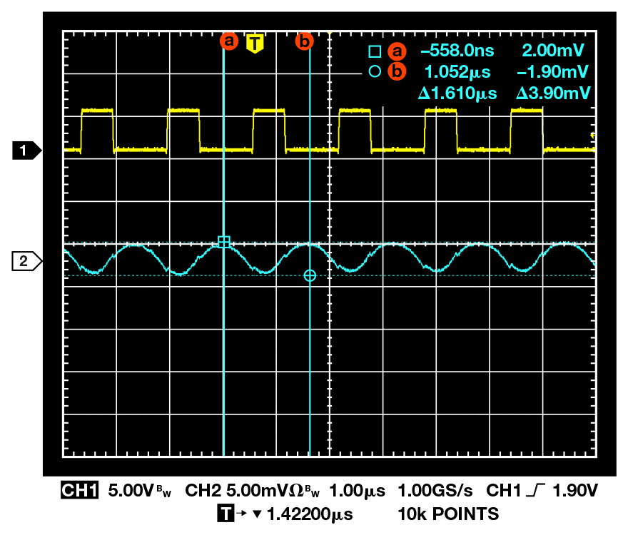
A comparison of the techniques shows that the coaxial cable in a 50-Ω environment provides more accurate results with less noise, even with a 500-MHz bandwidth. Changing the scope bandwidth to 20 MHz removes the high frequency noise, as shown in Figure 12. The ADP2114 generates an output ripple of 3.9 mV p-p in the time domain, which closely correlates with the measured value of 4 mV p-p using the 20-MHz bandwidth setting in the frequency domain.
 |
||
| Figure 12. | Switch node (1) and output ripple (2). | |
Measuring Switching Transients
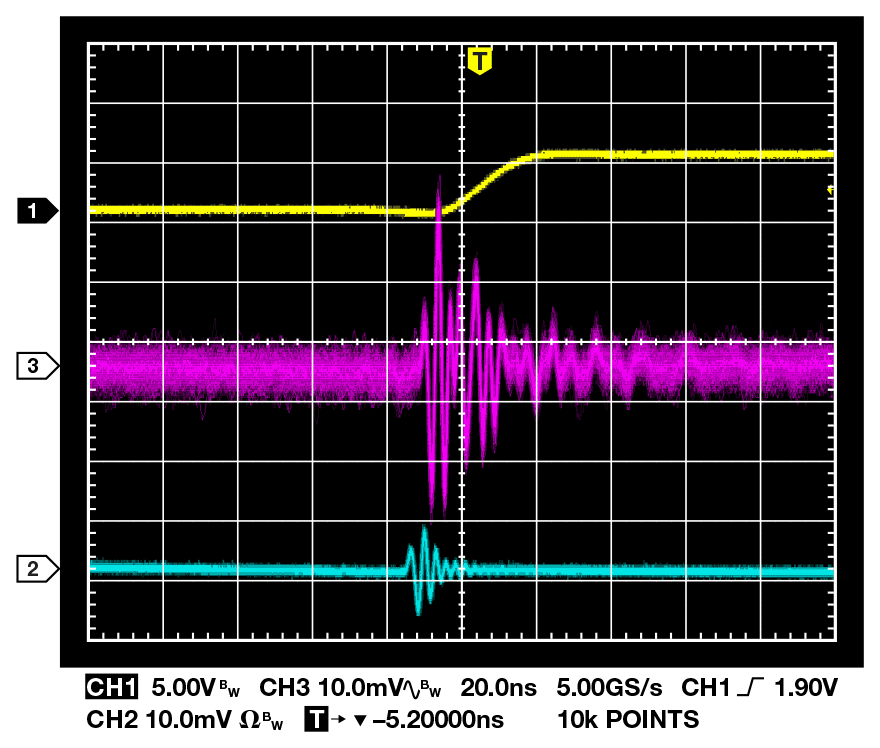
Switching transients have lower energy but higher frequency content than output ripple. This occurs during switching transitions and is often standardized as a peak-to-peak value including the ripple. Figure 13 shows a comparison of switching transients measured using a standard oscilloscope probe with long ground lead and a 50-Ω coaxial termination in a 500-MHz bandwidth. Typically, the ground loop due to the long ground lead generates larger switching transients than expected.
 |
||
| Figure 13. | Switch node (1), standard oscilloscope probe (3), and 50-Ω coaxial termination (2). |
|
Conclusion
Output ripple and switching transient measurement techniques are important to consider when designing and optimizing the system power supply for low-noise, high-performance converters. These measurement techniques provide an accurate, reproducible result in both time and frequency domains. It is important to maintain a 50-Ω environment when measuring low-level signals over a wide range of frequencies. A simple, low-cost way to do this is to use a 50-Ω coaxial cable that is properly end terminated. This method can be used with a wide range of switching regulator topologies.
References
- Power Management
- Switching Regulators
- Limjoco, Aldrick. AN-1144 Application Note. Measuring Output Ripple and Switching Transients in Switching Regulators. Analog Devices, Inc., 2013.
- Application Note 01-08-01, Rev. 01. Output Ripple Voltage Measurements. SynQor.
- Williams, Jim. Application Note 70. A Monolithic Switching Regulator with 100 µV Output Noise. Linear Technology, 1997.