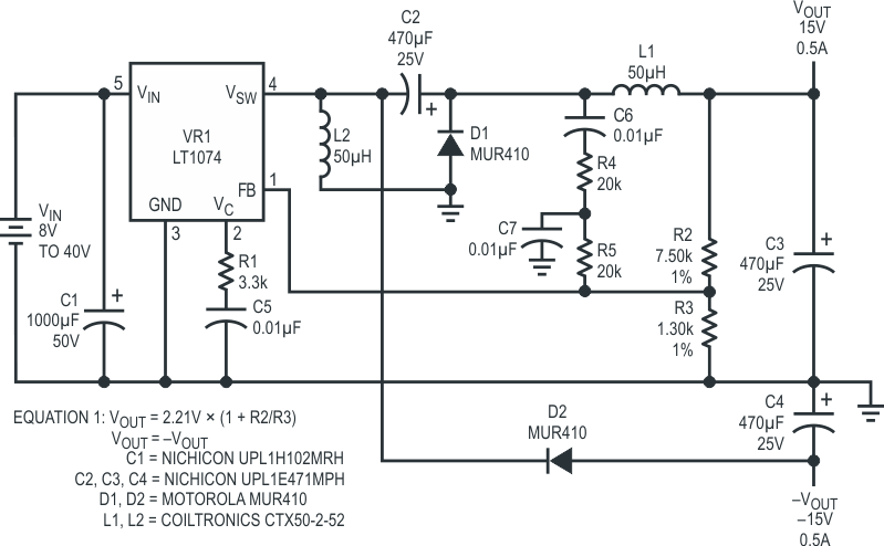
Many systems derive ±15 V supplies for analog circuitry from an input voltage that may be above or below the 15 V output. The split supply requirement is usually fulfilled by a switcher with a multiple-secondary transformer or by multiple switchers. An alternative approach, shown in Figure 1, uses an LT1074 switching regulator IC, two inductors and a “flying” capacitor to generate a dual-output supply that accepts a wide range of input voltages. This solution is particularly noteworthy because it uses only one switching regulator IC and does not require a transformer. Inductors are preferred over transformers because they are readily available and more economical.
 |
|
| Figure 1. | Schematic diagram for ±15 V version. |
The operating waveforms for the circuit are shown in Figure 2. During the switching cycle, the LT1074’s VSW pin swings between the input voltage (VIN) and the negative output voltage (–VOUT). (The ability of the LT1074’s VSW pin to swing below ground is unusual – most other 5-pin buck switching regulator ICs cannot do this.) Trace A shows the waveform of the VSW pin voltage and Trace B is the current flowing through the power switch.
 |
|
| Figure 2. | LT1074 switching waveforms. |
While the LT1074 power switch is on, current flows from the input voltage source through the switch, through capacitor C2 and inductor L1 (Trace C), and into the load. A portion of the switch current also flows into inductor L2 (Trace D). This current is used to recharge C2 and C4 during the switch OFF time to a potential equal to the positive output voltage (VOUT). The current waveforms for both inductors occur on top of a DC level.
The waveforms are virtually identical because the inductors have identical values and because the same voltage potentials are applied across them during the switching cycles.
When the switch turns off, the current in L1 and L2 begins to ramp downward, causing the voltages across them to reverse polarity and forcing the voltage at the VSW pin below ground. The VSW pin voltage falls until diodes D1 (Trace E) and D2 (Trace F) are forward biased. During this interval the voltage on the VSW pin is equal to a diode drop below the negative output voltage (–VOUT). L2’s current then circulates between both D1 and D2, charging C2 and C4. The energy stored in L1 is used to replace the energy lost by C2 and C4 during the switch ON time. Trace G is capacitor C2’s current waveform. Capacitor C4’s current waveform (Trace F) is the same as diode D2’s current less the DC component. Assuming that the forward voltage drops of diodes D1 and D2 are equal, the negative output voltage (–VOUT) will be equal to the positive output voltage (VOUT). After the switch turns on again the cycle is repeated.
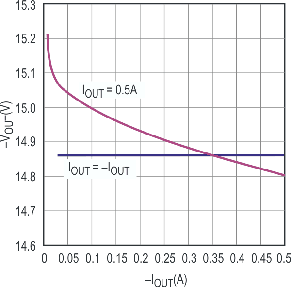
Figure 3 shows the excellent regulation of the negative output voltage for various output currents. The negative output voltage tracks the positive supply (VOUT) within 200 mV for load variations from 50 mA to 500 mA. Negative output load current should not exceed the positive output load by more than a factor of 4; the imbalance causes loop instabilities. For common load conditions the two output voltages track each other perfectly.
 |
|
| Figure 3. | –15 V output regulation characteristics. |
Another advantage of this circuit is that inductor L1 acts as both an energy storage element and as a smoothing filter for the positive output (VOUT). The output ripple voltage has a triangular waveshape whose amplitude is determined by the inductor ripple current (see trace C of Figure 2) and the ESR (effective series resistance) of the output capacitor (C3). This type of ripple is usually small so a post filter is not necessary.
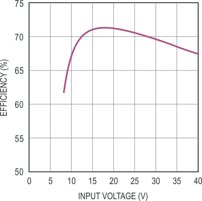
Figure 4 shows the efficiency for a 0.5 A common load at various input voltages. The two main loss elements are the output diodes (D1 and D2) and the LT1074 power switch. At low input voltages, the efficiency drops because the switch’s saturation voltage becomes a higher percentage of the available input supply.
 |
|
| Figure 4. | ±15 V efficiency characteristics with 0.5 A common load. |
The output voltage is controlled by the LT1074 internal error amplifier. This error amplifier compares a fraction of the output voltage, via the R2 to R3 divider network shown in Figure 1, with an internal 2.21 V reference voltage and then varies the duty cycle until the two values are equal. The RC network (R1 and C5 in Figure 1) connected to the VC pin along with the R4/R5 and C6/C7 network provides sufficient compensation to stabilize the control loop. Equation 1 can be used to determine the output voltage.
 |
|
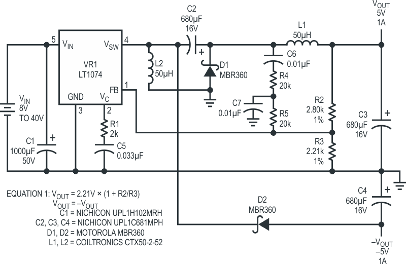
| Figure 5. | Schematic diagram for ±5 V version. |
Refer to the schematic diagram in Figure 5 for modified component values to provide ±5 V at 1 A.
 |
|
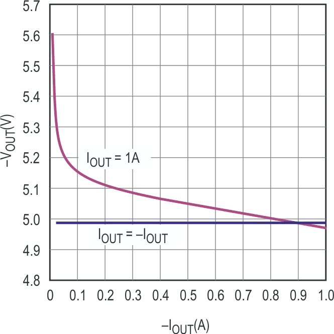
| Figure 6. | –5 V output regulation characteristics. |
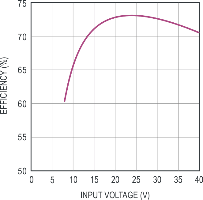
Figure 6 shows the circuit’s –5 V load regulation characteristics and Figure 7 shows its efficiency.
 |
|
| Figure 7. | ±5V efficiency characteristics with 1 A common load. |