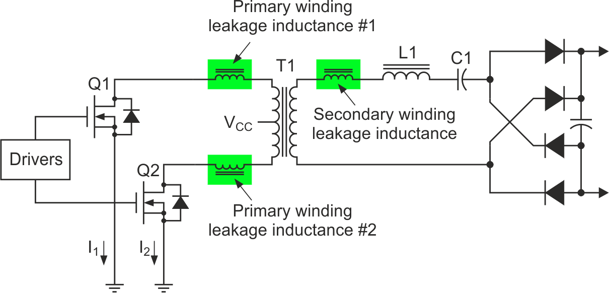
I worked on a quasi-resonant energy converter, which in an extremely simplified form looked like the one shown in Figure 1.
 |
||
| Figure 1. | This is a simplified design for a quasi-resonant push-pull inverter. | |
A push-pull pair of power MOSFETs would turn on and turn off in the usual alternation and when each one would turn on, its drain to source current, IDS, would rise and fall back down again along a sinusoidal curve. That curve's contour was set by the series resonance of C1 with a net inductance, the sum of L1 plus the leakage inductance of T1's secondary winding plus the leakage inductance of whichever side of the primary winding was operating on that half cycle.
That waveform contour arose from an LC resonance, but because switching events were involved, the process was actually quasi-resonant.
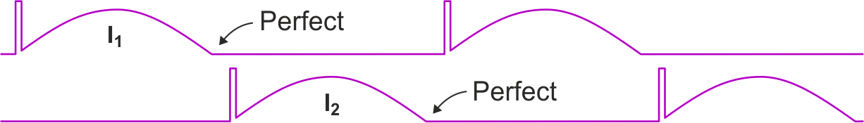
If the two halves of the primary winding had been exactly alike, their leakage inductances would be exactly alike too and the two current waveforms, I1 and I2, would be exactly alike, albeit at 180° phasing. If the resonances were just so, each MOSFET would get turned off at exactly the instant that the IDS of that MOSFET had come back down to zero (Figure 2).
 |
||
| Figure 2. | This diagram shows ideal, quasi-resonant switching. | |
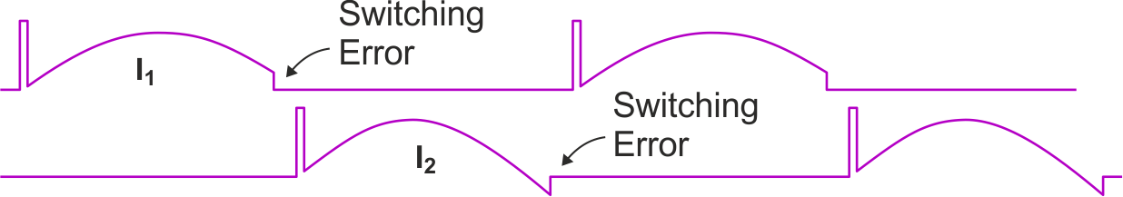
The fly in the ointment was that the two halves of the primary winding were not exactly alike. From the way that they had been constructed, their leakage inductances were ever so slightly different, which led to switching errors as in the Figure 3.
 |
||
| Figure 3. | Inconsistent leakage inductances cause switching errors. | |
If a leakage inductance were larger than nominal, the IDS would not yet have gotten down to zero when that side's MOSFET got turned off as with I1. On the other hand, if a leakage inductance were smaller than nominal, the IDS would not only have reached zero, it would have started flowing in the opposite direction until the MOSFET got turned off as with I2.
In our actual unit, we could adjust the drive frequency a little, but bringing one side of the circuit to "perfect" left the other side with a substantial "switching error." Trying to strike a compromise between the two sides wasn't deemed good enough either.
Our original C1 was 0.068 µF and our target LC-resonance was 100 kHz. From the standard resonance equation, the sum of the described inductances, accounting for T1's turns ratio of course, was 37.25 µH, most of which was provided by L1 but the switching imbalance and the resultant switching errors were thought to be too severe.
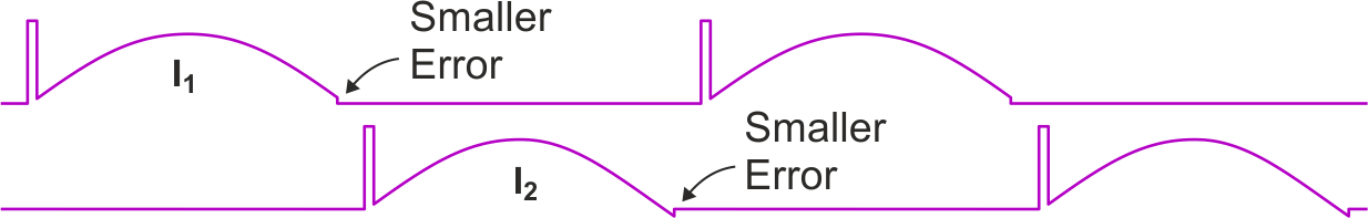
We lowered the value of C1 from 0.068 µF to 0.022 µF for which the inducatance target rose and became 115.1 µH. We made L1 of an apprpropriately higher inductance and got the results shown in Figure 4.
 |
||
| Figure 4. | The adjustments led to reduced switching errors. | |
We could never entirely eliminate the switching errors because the two halves of the T1 primary were still ever so slightly imbalanced. We were able however, to reduce those switching errors to being tolerably small.