EMI is a plague upon power electronic design architectures, and it can be mitigated in numerous ways. Adding an EMI filter may seem like the most obvious choice, but there may be a better first step.
Modern electronic power system architectures are becoming denser with a huge amount of interconnections. And reducing EMI in these kinds of systems is becoming increasingly challenging.
One of the top EMI offenders is the switched-mode power supply (SMPS). It can reside externally from a system design or printed circuit board (PCB) or it may be a part of a design on a PCB. Either way, EMI mitigation must be reduced in order to pass standards tests as well as operate surrounding circuitry without errors. This article will provide circuit designers with some of the best methods to control EMI in their designs.
The SMPS
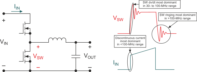
Due to its marked improvement in efficiency over linear regulators, the SMPS has become a crucial component in many system designs. The switching of the power silicon MOSFETs or GaN power devices, resulting in discontinuous currents, are the major offenders that can affect reliable system operation (Fig. 1). The following sections [#55] will outline some of the best ways to reduce the various forms of EMI.
 |
|
| Figure 1. | This schematic shows the EMI sources in an SMPS. (Image from Reference 8). |
Conducted EMI reduction methods
Conducted noise [6] is easier to analyze than radiated noise; designers can employ standard circuit analysis methods. However, many of the components in EMI analysis are parasitic and will not appear on a schematic diagram.
When power switching devices operate on and off, they will generate large discontinuous currents. These currents will appear at the input of a buck converter, the output of a boost converter, and at both the input and output of flyback and buck-boost converter designs.
Discontinuous currents will generate voltage ripple that may be conducted to other parts of the system architecture through conductors coming in contact with each other. Such currents at the converter input should be filtered through an input filter to mitigate voltage disturbances. The output of the power converter also may need a filter to help pass EMI standards.
Common-mode noise is typically more difficult to analyze because it’s usually caused by charge/discharge of parasitic capacitances, which are highest in a heatsink or a transformer interwinding capacitance.
Radiated EMI reduction methods
Radiated noise [5] can be evaluated in two ways:
- Electromagnetic noise measured with an antenna some meters away.
- Magnetic noise measured with a “sniffer probe” close to the magnetic components.
The origin of an electromagnetic field is typically a current containing high-frequency harmonics that are flowing in a loop. Reducing the loop area, the di/dt, or the current peak amplitude will help reduce radiated noise.
Dithering in Switching Voltage Regulators
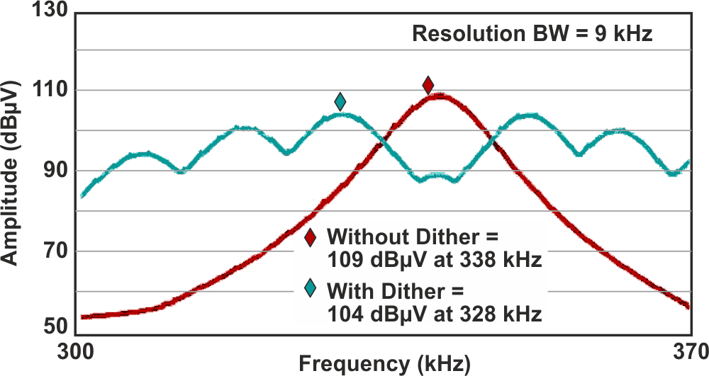
Dithering switching-voltage-regulator switching frequency – through the use of spread-spectrum frequency-modulation (SSFM) techniques – will reduce EMI and help designers pass compliance testing when filtering and optimized layout fails to meet EMI standards limits. Dithering [1] slightly modulates a fundamental switching frequency in the switching regulator. Here’s how it works.
The electromagnetic emissions of a switch-mode power supply are spread across many frequencies via a square-wave pulse, where the greatest energy is at the fundamental frequency. Slightly varying the fundamental frequency (using a typical modulation of 3% or so) would modulate the peak switching noise energy, which would be shared among multiple fundamental frequencies. The total electromagnetic energy will remain the same, but the narrowband energy has been decreased so EMI is effectively reduced.
In the example shown in Figure 1, 5-dB peak noise reduction can make all the difference between a fast time to market with standards approval or a lengthy effort to lower noise peaks below standards limits (Fig. 2).
 |
|
| Figure 2. | This graph demonstrates quasi-peak measurements with and without dithering around 330 kHz, showing a 5-dB reduction due to dithering. (Image from Reference 1). |
Using Packaging and Pinout to Lower EMI
Many designers may not think about the benefits of selecting a type of IC packaging that can help lower EMI. One great example is packaging for a power MOSFET in a fast SMPS. These kinds of power converters use fast switched voltage slew rates (dv/dt) as well as high current rates (di/dt) that will increase EMI in a system.
Designers can add an EMI filter as a solution. However, before doing that and adding to the size of a design (thus lowering power density), take a look at package technologies that also may help mitigate EMI. What follows are some examples of how to improve EMI with a power MOSFET package design.
Setting up parallel pins for the input power and GND pins will enable symmetrical placement of high frequency input capacitors. In addition, equivalent parasitic loop inductance of the two equal and parallel inductances are halved.
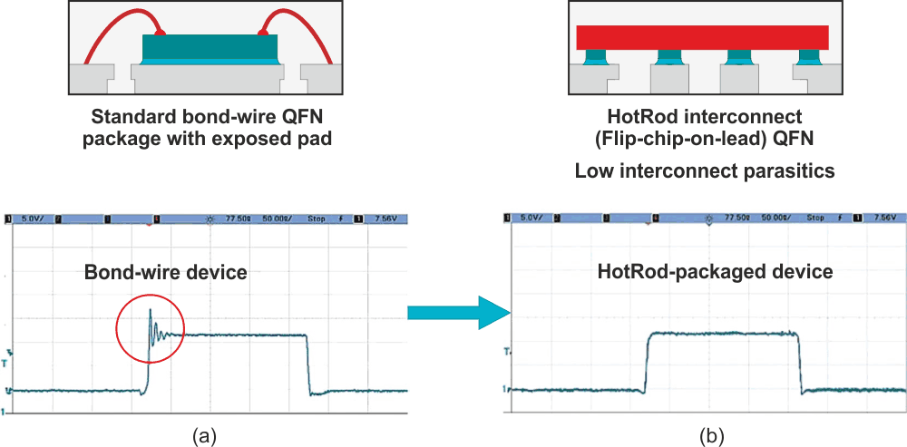
Bond wires in a QFN package can sometimes be eliminated via the use of copper pillars and a flip-chip interconnection between the lead frame and the die (Fig. 3).
 |
|
| Figure 3. | This typical QFN package uses bond wires to connect the die to an exposed pad where the power switch exhibits significant ringing (a). An improved package utilizes copper pillars and a flip-chip interconnection from the die to the lead frame, which eliminates a ringing in the power switch (b). (Image from Reference 8). |
Circulating input currents will create opposing magnetic fields that result in H-field cancellation and reduced radiated emissions. So, by creating a symmetric layout of high di/dt input loops, the magnetic fields generated (of opposing directions) can cancel each other.
Another way to reduce EMI for the package is to place a continuous ground plane for return current beneath the two inductor loops on another PCB layer, such as layer 2, which is right below the top layer power circuit.
The EMI Filter
EMI filters may be discrete or modular in design. Power designers will have to choose which is most beneficial to their design needs in terms of time, size, and cost.
EMI filters in a high-power-density power-supply architecture
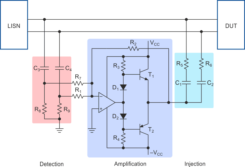
It’s essential to minimize the size of an EMI filter in a high-power-density power supply. [7] A filter design that has no magnetic components is more compact, thus achieving good power density.
For instance, the filter design in Figure 4 uses voltage detection and a current injection topology without magnetic components. To enhance the output current and power of the filter as well as improve insert loss (IL), a push-pull power-amplifier circuit is used behind the output of the amplifier so that the output current is large enough. This filter design is stable enough to replace a passive EMI filter.
 |
|
| Figure 4. | This high-performance filter design, with no magnetic components, can support high output currents in the order of 60 A. (Image from Reference 7). |
Shielding an EMI filter as a last-ditch effort to control conducted EMI
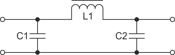
A differential-mode (DM) EMI filter (Fig. 5) may produce conducted EMI interference in a power-supply system.
 |
|
| Figure 5. | Shown is a Pi-type EMI filter (Image from Reference 9). |
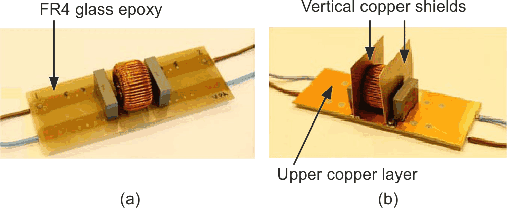
A copper shield [9] placement below the DM filter may help (Fig. 6a). When all else fails, add copper layers to the top and bottom of the PCB plus two vertical copper shields on either side of the filter (Fig. 6b).
 |
|
| Figure 6. | Two different configurations for the DM EMI filter: In (a), the filter is on top of a single- copper-layer PCB with a distance of 3.5 mm between each of the filter components. In (b), the filter is atop a double-copper-layer (top and bottom) PCB and two vertical copper shields, with 3.5 mm between each of the filter components. (Image from Reference 9) |
Summary
Designers need an understanding, as well as the tools, to minimize both conducted and radiated EMI disturbances to and from their board design. This article has focused on the SMPS, which greatly improves efficiency over linear supplies, but also can become a time-consuming effort to minimize EMI disturbances. The techniques and tools presented here offer ways to improve an SMPS design to help the architecture pass EMI standards tests while minimizing design time, too.
References
- Understanding Noise-Spreading Techniques and their Effects in Switch-Mode Power Applications, TI Power supply design seminar
- An overview of conducted EMI specifications for power supplies
- An overview of radiated EMI specifications for power supplies
- Enhanced HotRod QFN Package: Achieving Low EMI Performance in Industry’s Smallest 4-A Converter
- Reducing EMI in switch mode power supplies
- Simple success with conducted EMI from DC-DC converters
- Research of active EMI suppression strategy for high power density power supply, IEEE Xplore
- Time-Saving and Cost-Effective Innovations for EMI Reduction in Power Supplies
- Effect of shielding and component placement in DM EMI filters on a power supply’s conducted EMI, IEEE Xplore