Introduction
A PCB is designed using a number of elements and components, each component holding a specific function that contribute to the application of the entire circuit. A very important component you should not overlook is the layout of your PCB. A good engineer will always make sure his layout provides the best functionality possible. Having a well configured layout will also reduce the chances of error. In this article we will discuss some layout tips that will help you in your PCB projects.
Sizing your Copper Traces
The copper traces used in PCB layout have some resistance. This resistance is not constant but depends on the length, thickness and width of the copper trace. Whenever current passes through a trace, it will experience a voltage drop, power dissipations and a rise in temperature. Resistance is defined by:
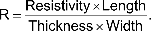 |
In order to control the resistance, focus on the size of the trace i.e. its length, thickness and width etc. We measure PCB trace thickness in ounces of copper. One ounce of copper is means 1 oz. of copper over an area of 1 square foot area. This thickness is equal to 1.4 thousandths of an inch. Usually 1-2 oz. copper is used but 6 oz. is also available. You can use a PCB trace width calculator to calculate the width and thickness of your traces with respect to its application. Try to keep a 5 °C temperature rise. If you have extra space then use larger traces in your layout. Also keep in mind that the inner layers will heat up more than the outer layers.
Making Loops Smaller
Try to keep your loops as small as possible. Specifically frequency loops. Keeping your loops small will reduce resistance and inductance and high frequency voltage spikes caused by
You can further reduce inductance by placing loops over a ground plane. Smaller loops will also reduce the inductive coupling of signals from external sources into nodes. This is if you aren’t designing an antenna.
Placement of Your Decoupling Capacitor
In order to maximize the decoupling efficiency, place you decoupling capacitors close to the IC; specifically between you power and ground source. If you place your capacitors away then there is a chance unwanted inductances could get generated. You can reduce inductance by using multiple vias from the capacitor pin to the ground plane.
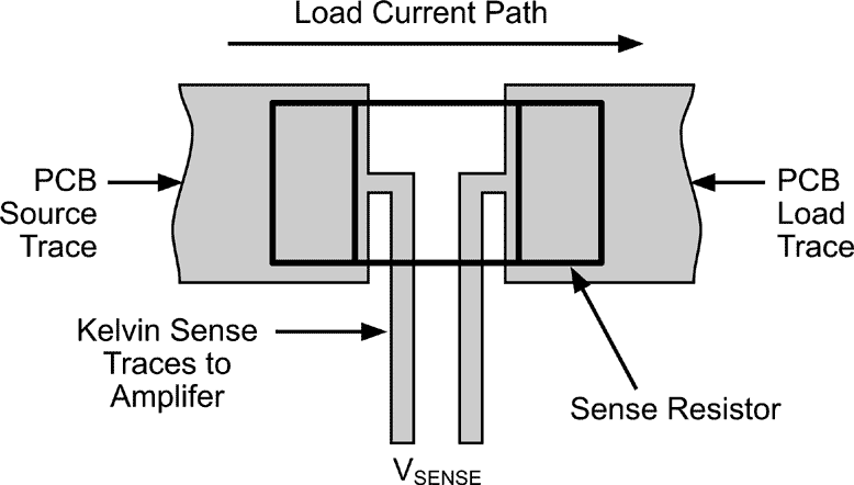
Correct Kelvin Connections
Kelvin connections are used to make electric potential contact with a current carrying component that reduces or eliminates the effect of contact resistance. Kelvin connections are useful in measurements and are made in a way to reduce stray resistances and inductance. If you don’t use Kelvin connections then the traces on the schematic placing could put your measurements off due to inductance and resistance.
Keeping Noisy Traces Away from Analog Traces
You should try to keep high frequency or noisy traces away from analog traces. If they are placed close together then the signals on the traces will capacitively couple especially in parallel traces.
Grounding your PCB
You should always make your ground trace large so the currents can be directed properly, for example, to direct noisy signals away from quiet signals. Ideally, you should place a ground place directly under signal traces to lower the impedance.
Via Sizing and Numbering
Remember that your vias have inductance and resistance and you should try to keep the inductance and resistance as low as possible. For this, use multiple vias and larger vias. You can use via size calculator too.
Using PCB as a Heatsink
Using extra copper around the components can increase the surface area of your device and allow more heat dissipations. This can turn your PCB surface into a heatsink. You should look into the components datasheet for further guidelines.
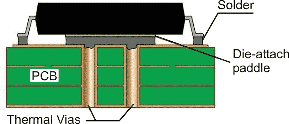
Using Thermal Vias
Using thermal vias will help in heat dissipation. You should try to use larger vias to transfer more heat and try to increase efficiency by lowering the operating temperature. A lower operating temperature will consequently increase the reliability.
Creating Thermal Relief
Making small connections between a trace and a component pin will create thermal relief. This will reduce the impact on electric resistance.
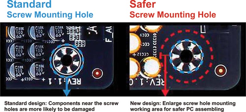
Distancing between Traces and Mounting Holes
You can reduce the effects of shock hazard by leaving space between the copper traces and mounting holes. Also make sure there is space between copper and any mounting components.
Placing your Heat Sensitive Components
Try to keep heat generating components away from heat sensitive components. Some heat sensitive components include thermocouples, electrolytic capacitors. If you place thermocouples near heat sources then your temperature measurements will be inaccurate and if you place electrolytic capacitors near heat sources can reduce their operating life. The heat is usually generated by passing current. Some heat generating components include bridge rectifiers, diodes, inductors etc.
PCBGOGO Quick Turn PCB Fabrication and PCB Assembly Manufacturer