by Kevin
DesignSpark PCB is the world’s most accessible electronics design software, specially designed for rapid prototyping and turning your circuit ideas into testable boards faster. It is offered free of charge for companies, hobbyists, educators and more.
I explored the new features of DSPCB v9.0, these features all target improving operation and reducing the chance of user errors providing both convenience and confidence. The features I appreciated the most include: detecting dangling connections in the schematic, adding a copper pour to a net within the pour area, being able to create a new library when saving a component and a search/find window in the Goto bar. Other enhancements include text alignment with the cursor and improvements to the Excellon drill file which improves compatibility with various viewers.
 |
Dangling connection detection in schematics.
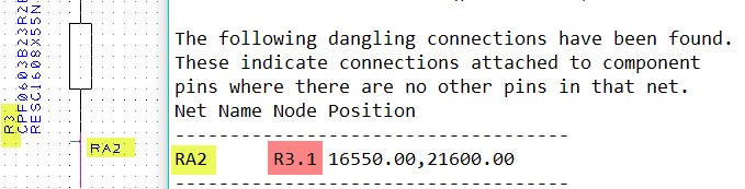
Something that has caught me out in the past is an incomplete net when using the shortcut of a named net at one IC pad but failing to terminate it at its destination. Result a missing track on the PCB! Yes, it could have been found with the existing reports and checks, but I missed it. Now in version 9, we have an additional method the “Dangling Connections” report for the schematic sheet (Figure 1).
 |
|
| Figure 1. | DesignSpark PCB V9.0 now have an additional method the “Dangling Connections” report for the schematic sheet. |
This is different from the unconnected pins report which reports every pin not connected and should be used as an additional part of your design checking process.
Net selection in copper pour areas.
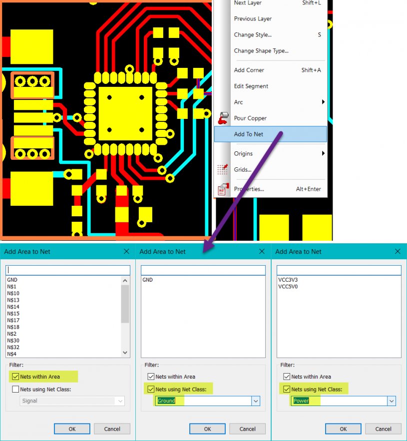
Another area I have had issues with previously is using a split power plane using copper pours. Having multiple pour areas for digital control, analog signal conditioning and power switching it can be easy to select the wrong net when viewing a long list of nets to connect to. Now have the choice to select nets that exist only within the selected pour area and further reduce the net options by filtering by the net class. Selecting a net from a list of two or three net names provides focus compared with selecting a net from 50 or so nets.
 |
|
| Figure 2. | DesignSpark PCB V9.0 now have the choice to Net selection in copper pour areas. |
Text alignment and style options.
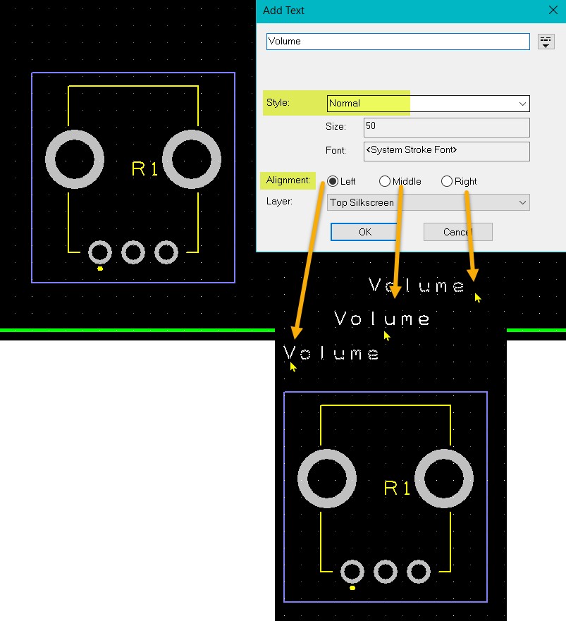
We can now “Add Text” with selecting the text styles available in the Design Technology and alignment relative to the cursor, this is useful for annotating the silkscreen or documentation layouts and can make a consistent and neat layout easier to produce (Figure 3).
 |
|
| Figure 3. | DesignSpark PCB V9.0: Text alignment and style options. |
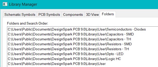
Save component to a new library.
The new option to create a “New Library” when saving (also copy and move) a component can help with creating a more structured library. This is very useful for building up libraries of components of common types (Figure 4).
 |
|
| Figure 4. | DesignSpark PCB V9.0: Save component to a new library. |
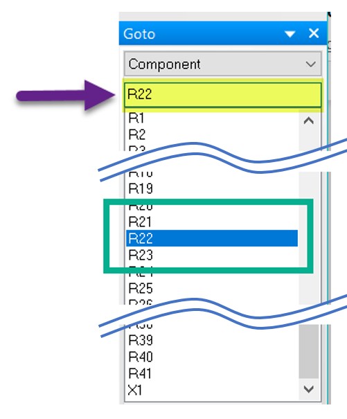
Goto bar selection aid.
The new selection box in the Goto bar helps to find things quickly without scrolling up and down the list (Figure 5). Start typing the item name and the list dynamically scrolls below and highlights the component once completely identified. I found this useful for both components and nets.
 |
|
| Figure 5. | DesignSpark PCB V9.0: Goto bar selection aid. |
Excellon drill file enhancements.
The Excellon drill file is also improved, a small change which has a big impact is the coordinates now contain a decimal point. This makes the file ‘more’ human readable but also appears to make the Gerber Viewers and FlatCAM work without having to change the FlatCAM Preference for the format. If the decimal point is present in the .drl file this overrides the format settings defined in FlatCAM, so no more fiddling around setting the data format in FlatCAM.
I would like to remind you that in general DesignSpark PCB CAD software is offered absolutely free and has a number of advantages:
- Seamless integration into existing design workflows.
Our range of free-of-charge design tools and resources take your brightest ideas all the way through to final production. Whether you're looking for a design alone tool, a range of technical information, a complete design ecosystem, our complete suite can be integrated seamlessly in to your existing design workflow.
- No limitation on your schematic size.
Be free when creating your schematic – there is no limitation on your schematic size or number of your schematic sheets.
- No limitation on your PCB design.
Feel free to use as many layers as you need on your next PCB design. There are no limits on the maximum number of nodes or pads and no restriction on the number of connections. The maximum size your PCB can be is 1 m × 1 m - Create your own libraries or use ours.
You can create your own part models in the library editor or access our ready to use embedded libraries. You can also use our new online tools to obtain models of the parts you need.
- Output the files you want.
Prepare unrestricted Gerber and ODB++ files to order PCBs from your favourite PCB manufacturer or let our PCB Quote service build it quickly for you
- Create BOMs in the format you want.
Prepare a Bill of Materials in the format you want and order the parts you need when you need them. You can quickly upload your BoM to the RS Components website using BOM-Quote service and let us find the parts for you.
- Integration with PCB Part Library.
Can't find a model of the part that you require, we also provide an additional tool that will allow you to quickly create them.