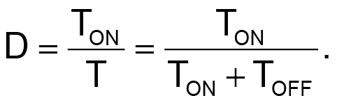
Switching regulators use a duty cycle to realize voltage or current feedback control. The duty cycle is the ratio of the turn-on time (TON) to the complete cycle length, the turn-off time (TOFF) plus on time, and defines a simple relationship between the input voltage and an output voltage.
 |
||
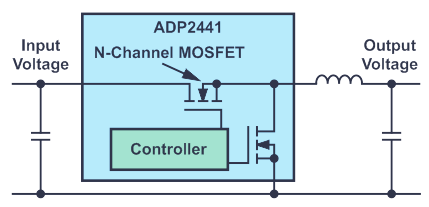
| Figure 1. | A typical step-down switching regulator with an ADP2441. | |
Other factors may be considered for a more exact calculation, but they are not decisive in the following explanations. The duty cycle of a switching regulator depends on the respective switching regulator topology. A step-down (buck) converter, as shown in Figure 1, has a duty cycle D according to
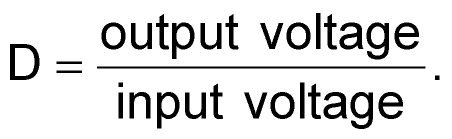
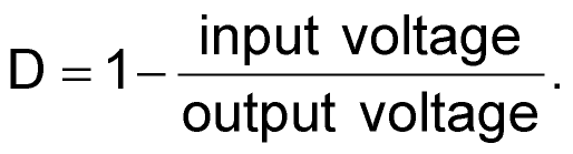
For a step-up (boost) converter, the duty cycle
These relationships apply to continuous conduction mode (CCM). Here, the inductor current does not drop to 0 in a time period, T. This mode is frequently found in circuits with operation at rated load. At lower loads or for intentional intermittent operation, the coil current discharges during the off time. This mode is called discontinuous conduction mode (DCM). These two modes of operation each have their own relationships for the respective duty cycle for a specific input voltage and output voltage.
Figure 2 shows an example of switching behavior in the time domain. Here we consider a step-down switching regulator in nonintermittent operation mode; that is, in continuous conduction mode. The duty cycle is independent of the switching frequency. The period T typically lies between 20 µs (50 kHz) and 330 ns (3 MHz). If the values for input voltage and output voltage are the same, a duty cycle of 1 is needed. This means that there is only an on time and no off time. However, this is not possible with every switching regulator. In Figure 1, the high-side MOSFET would have to be continuously on for this. If this switch is designed as an N-channel MOSFET, it needs a higher voltage at the gate than the input voltage of the circuit in order to operate. If there is a certain off time after each on time, as is the case for a duty cycle of < 1, a higher voltage than the supply voltage can be generated quite easily according to the charge pump principle. However, this is not possible with a duty cycle of 100%. Thus, for switching regulators with 100% duty cycle capabilities, either elaborate charge pumps acting independently of the switching regulator MOSFETs must be implemented or the high-side switch shown in Figure 1 must be designed as a P-channel MOSFET. Both also result in additional effort and cost.
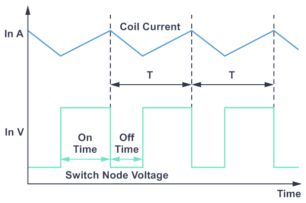 |
||
| Figure 2. | Time domain representation of switching in a step-down switching regulator with coil current in CCM. |
|
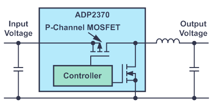
Figure 3 shows a switching regulator, the ADP2370, that permits a 100% duty cycle through use of a P-channel MOSFET as the high-side switch. For this type of buck converter, the input voltage can drop to very near the output voltage. With the P-channel switch integrated into the switching regulator, additional cost is avoided.
 |
||
| Figure 3. | Example of a switching regulator permitting a duty cycle of 100%. | |
If an application requires that the input voltage be able to drop to a level very close to the output voltage setpoint, a switching regulator that permits a duty cycle of 1, or 100%, should be selected.
Apart from this limitation on the duty cycle, determined by the high-side switch of a switching regulator topology, other limitations are imposed on the duty cycle. We will consider them in a later power management tip.