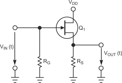
By using JFETs in unusual configurations, you can design simple, high-frequency LC oscillators with few passive components. The structure for implementing the amplifier stage comprises a JFET transistor that you configure as a common drain (Figure 1).
 |
|
| Figure 1. | You can configure an amplifier stage, based on a JFET transistor, as a common drain. |
When the JFET transistor works in the saturation zone, the drain current, ID, is:
where IDSS is the maximum saturation current and VP is the pinch-off voltage. You can model the JFET in this saturation zone in the small-signal regime using an infinite input impedance and a current source that the gate-source voltage controls. The following equation determines the small-signal transconductance of the transistor:
Gate resistance RG provides the necessary connection from the gate to ground. Its typical value is in the low-megaohm range to provide the needed high impedance of the amplifier structure. Resistance RS biases the transistor; the following equation determines resistance:
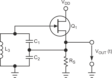
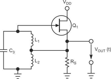
To complete the oscillator circuit, you add an LC-resonant tank to the amplifier stage (Figure 2); the result is a Colpitts oscillator. The connection from the gate to ground for dc exists because of the inductance of the LC-resonant tank, removing the gate resistance of the amplifier.
 |
|
| Figure 2. | To complete the oscillator circuit, you add an LC-resonant tank to the amplifier stage; the result is a Colpitts oscillator. |
Analyzing the circuit using the Barkhausen criterion, the frequency of oscillation fO of the circuit is:
The necessary condition on the capacitors so that the circuit can oscillate is:
or, equivalently, the voltage gain, AV, of the amplifier stage, VOUT(t)/VGS(t), is:
where voltage gain of the common drain stage is:
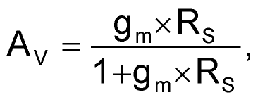
which demonstrates that the voltage gain is always lower than one.
 |
|
| Figure 3. | You can develop a Hartley oscillator based on a JFET transistor. |
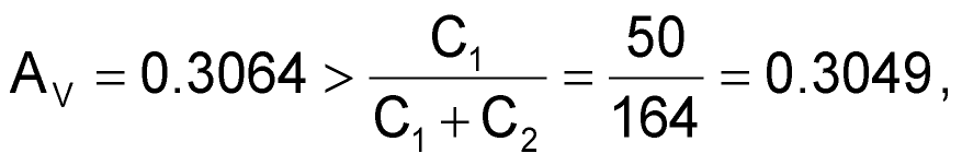
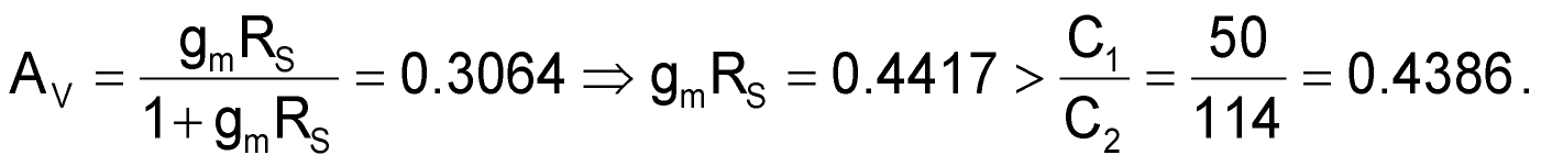
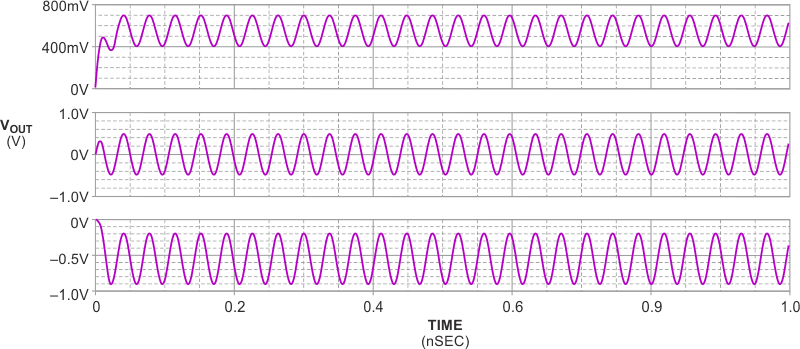
Similarly, you can develop a Hartley oscillator based on a JFET transistor (Figure 3). The simulation and experimental results for the Colpitts oscillator circuit uses a 2N3819, an n-channel device, for the JFET. The PSpice parameters for this transistor are IDSS of 12 mA and VP of –3 V. Simulation shows the voltage gain of the amplifier circuit is 0.3064, and, with C1 having a value of 50 nF and C2 having a value of 114 nF, then
and the circuit oscillates (Figure 4), which also shows the start-up process of the oscillator. The voltage gain also shows that the design meets the start-up conditions on the capacitors:
 |
|
| Figure 4. | With C1 having a value of 50 nF and C2 having a value of 114 nF, the circuit oscillates. |
Note that transconductance of the transistor is equal to the value of the slope of the curve iD = f(VGS) at this operating point. Depending on this point, the actual value of the transconductance will be larger or smaller. Confirming this value, when oscillations start up, the curve iD = f(VGS) restricts the amplitude of the output signal due to the reduction of the transconductance when VGS decreases to values close to the pinch-off voltage; in this zone of the curve, its slope and, therefore, the transconductance is smaller. The intrinsic nonlinearity of the JFET transistor limits the gain of the amplifier stage, and no additional circuit stabilizing the amplitude of the output signal is necessary.