A Class D amplifier provides better efficiency and thermal performance than a comparable Class AB amplifier, but implementing a Class D amplifier still requires attention to good electrical- and thermal-design practices. Most engineers use a continuous-sine-wave-input signal to evaluate a Class D amplifier's performance in the lab. Although convenient for measurement purposes, a sine wave represents a worst-case scenario for the amplifier's thermal load. If you drive a Class D amplifier near maximum output power with a continuous sine wave, it's not uncommon for the amplifier to enter thermal shutdown.
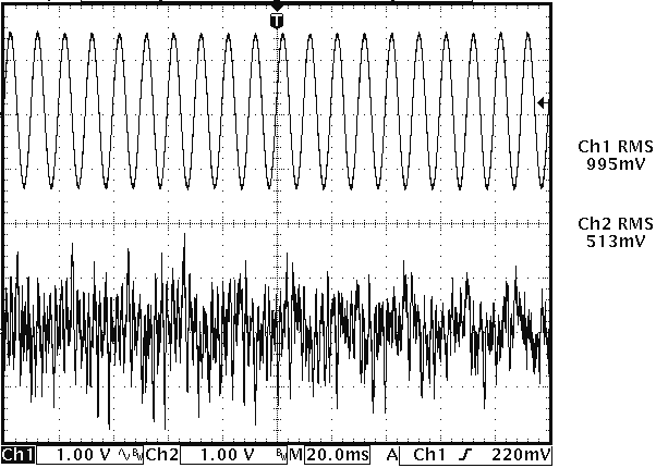
Typical audio-program material comprising music and voice has a much lower rms value than its peak output power. The ratio of peak-to-rms power, or “crest factor,” typically averages about 12 dB for voice and 18 to 20 dB for musical instruments. Figure 1 shows time-domain-oscilloscope, rms-voltage measurements of an audio signal and a sine wave. Although the audio signal corresponds to a burst of music, it presents a slightly higher peak value than the sine wave, and its rms value approaches only half and may average even less than that of the sine wave. An audio signal's thermal effects on a Class D amplifier are considerably lower than a sine wave's, and, thus, it's important to test performance with actual audio signals instead of sine waves.
 |
|
| Figure 1. | A sine wave’s higher rms level than that of an audio signal predicts the additional thermal burden on a Class D amplifier that’s tested with a sine wave. |
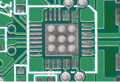
In an industry-standard TQFN package, a bottom-side-exposed pad provides the primary path for heat transfer from the IC and into copper areas of the amplifier's pc board that serves as a heat sink. Soldering the IC to a large copper pad helps minimize thermal resistance, as do multiple vias that transfer heat to the pc board's opposite side, on which an additional copper area further reduces thermal resistance. In addition, you can connect any of the device's pins to the thermal transfer area, provided that the pins and thermal pad are at the same electrical potential, such as the upper- and lower-right pins in Figure 2.
 |
|
| Figure 2. | The exposed tinned-copper pad in the center provides the primary thermal path for a Class D amplifier IC in a TQFN or TQFP package. |
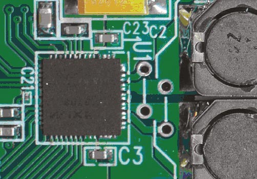
Although an IC's pins don't provide the primary heat-transfer path, they do dissipate a small amount of heat, and it's helpful to maximize the widths of all pc traces that connect to the IC. Figure 3 shows how wide traces connect the IC's outputs to two inductors. In this case, the inductor's copper windings provide an additional thermal path away from the Class D amplifier. Improving heat dissipation by even a few percentage points may make the difference between achieving acceptable performance and encountering thermal problems. To further reduce thermal resistance, you can specify a heat sink that solders to the pc board adjacent to the IC. For example, a Wakefield Engineering (www.wakefield.com) 218-series sink has lower edges that form the conduction path.
 |
|
| Figure 3. | The wide traces to the right of this Class D-amplifier IC help conduct heat away from the device and into the adjacent components. |
A few basic calculations can help you estimate a Class D-amplifier IC's die temperature. For example, consider an amplifier that operates at an ambient temperature of 40 °C, has output power of 16 W, and has 87% efficiency. Specified thermal resistance from the IC's junction to ambient air is 21 °C/W. First, calculate the Class D amplifier's power dissipation:
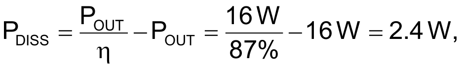
where PDISS is the dissipated power, POUT is the output power, and η is the efficiency. Use the power dissipation to calculate the die temperature, TC, as follows:

which is within the device's maximum junction temperature of 150 °C. A system seldom enjoys the luxury of operation at a 25 °C ambient temperature, and it's important to base these calculations on a reasonable estimate of the system's actual internal ambient temperature.
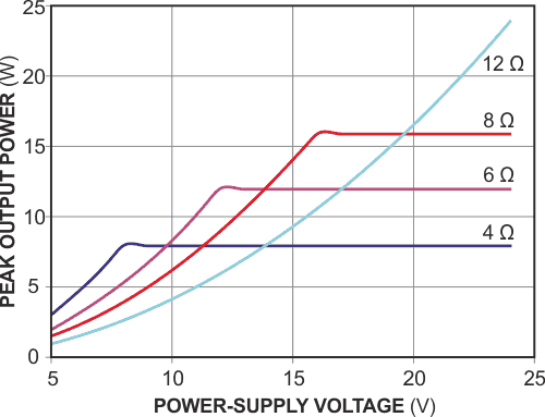
The on-resistance of a Class D amplifier's MOSFET output stage affects both its efficiency and its peak-current capability. Reducing the peak load current reduces the infinite-impulse-response losses and increases efficiency in the MOSFETs. To further lower peak currents, choose the highest impedance speaker that delivers the desired output power within the voltage-swing limits of the Class D amplifier and its supply voltage. In Figure 4, a Class D amplifier with an output-current capability of 2 A and a supply-voltage range of 5 to 24 V goes into current limiting with a 4 Ω load and a supply voltage of 8 V for a corresponding maximum continuous output of 8 W.
 |
|
| Figure 4. | Selecting an optimal impedance, such as 12 Ω, and supply voltage, such as 15 V, maximizes output power and prevents current-limiting- induced distortion. |
If 8 W represents an acceptable output power, consider using a 12 Ω speaker and a 15 V supply voltage. The peak current limit then occurs at 1.25 A, with a corresponding maximum continuous output power of 9.4 W. Furthermore, the 12 Ω load operates at 10 to 15% higher efficiency than the 4 Ω load and thus lowers the IC's power dissipation. Actual efficiency improvements vary among Class D-amplifier ICs.
 |
|
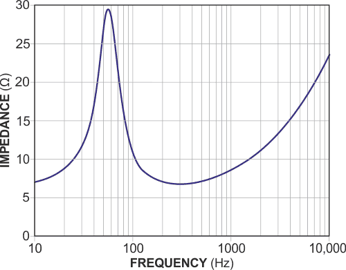
| Figure 5. | The electrical impedance of this nominally 8 Ω, 13-cm-diameter, wide-range loudspeaker varies significantly with frequency. |
To complicate matters for the designer, a loudspeaker behaves as a complex electromechanical system that presents a variety of resonances across its frequency range and exhibits its nominal impedance only within a narrow frequency band (Figure 5). Over much of its audio bandwidth, this loudspeaker's impedance exceeds its nominal value of 8 Ω; adding a crossover network and a tweeter may reduce the total load impedance below the nominal value. Keep the load impedance's behavior in mind when you consider the amplifier's power-supply current and thermal-dissipation capability.