Abstract
This article will explain the inherent limitations of the boost topology and how to overcome them. When designing and evaluating boost converters, sometimes the intended output voltage is not realized. Instead, it has a lower value than desired.
Introduction
Boost converters are used for generating high output voltages from low input voltages. Such a voltage conversion can easily be done with a switching regulator with a boost topology. However, the voltage gain has a natural limit. The voltage gain is the ratio of output voltage to input voltage. If 24 V is generated from 12 V, then the voltage gain is 2.
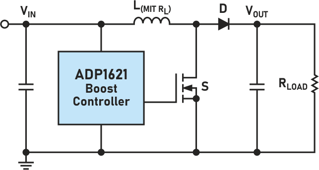
As an example, let’s look at an industrial application in which a voltage of 300 V should be generated with a 160 mA output current from a 24 V supply voltage (Figure 1).
 |
|
| Figure 1. | A boost converter circuit. |
The voltage gain can also be expressed in terms of the duty cycle, D:
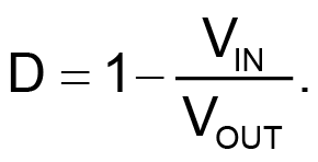 |
(1) |
The main parameters of a boost converter are the duty cycle and the voltage gain. The duty cycle indicates the amount of time that the switch, S, is on in each cycle. The voltage gain describes the factor by which the output voltage exceeds the input voltage.
To generate a high voltage, the duty cycle increases to values close to 1 but never reach 1.
By selecting a boost converter with a high maximum duty cycle, it may seem possible to generate a high output voltage from a low supply voltage. However, there’s more to it than that. Besides the duty cycle limits, the maximum possible voltage gain also must be taken into consideration.
The voltage gain describes the maximum possible output voltage of a boost converter in relation to the available input voltage. This limitation of the boost converter can be thought of in the following way: with the boost, all energy transferred from the input side to the output side must first be temporarily stored. During the on time – that is, when the switch, S, in Figure 1 is on – energy is temporarily stored in the inductor, L. At this time, the diode, D, in Figure 1 blocks the current flow.
During the off time, the temporarily stored energy is removed from the inductor, L. Both the charging and the discharging of the inductor must follow the rules of the inductance. The current flow in each case is determined by the inductance value of the inductor and the respective voltage difference across the inductor. The voltage across the inductor can be described simply as being VIN during the charging time and VOUT minus VIN during the off time.
With a high voltage gain, the off time may not be long enough for the temporarily stored energy to be recovered from the inductor. Thus, the simplified formula that describes the duty cycle in Equation 1 does not account for this limitation. The formula for the maximum voltage gain can only be recognized if the DC resistance (DCR) of the inductor and the load resistance are also taken into account. See Equation 2:
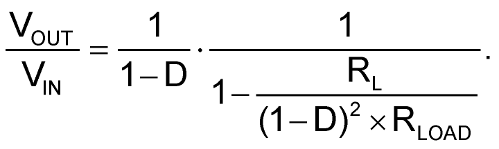 |
(2) |
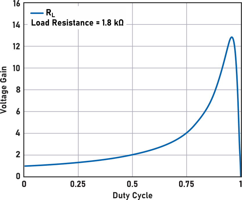
The ratio between RL and RLOAD therefore affects the ratio between the possible input and output voltages and thus, the voltage gain of a boost converter. This voltage gain can be illustrated in a diagram. Figure 2 shows the example with a 24 V input voltage and a 300 V output voltage at 160 mA for a load resistance of 1.8 kΩ and an inductor RL – that is, DCR – of 3 Ω.
 |
|
| Figure 2. | A possible voltage gain when the load resistance is 600 times as high as the DCR (RL) of the inductor. |
In this example, Figure 2 shows that it is possible to achieve a voltage gain of approximately 12.5 (derived using Equation 2). However, if the load resistance is lowered – that is, the output current is increased – or the DCR (RL) of the inductor is increased – that is, the inductor size is decreased – it will no longer be possible to produce the required voltage gain.
Figure 3 shows the curve of the voltage gain when the ratio between load resistance and inductor resistance is 300. Here, RL of 6 Ω and a load resistance of 1.8 kΩ were selected.
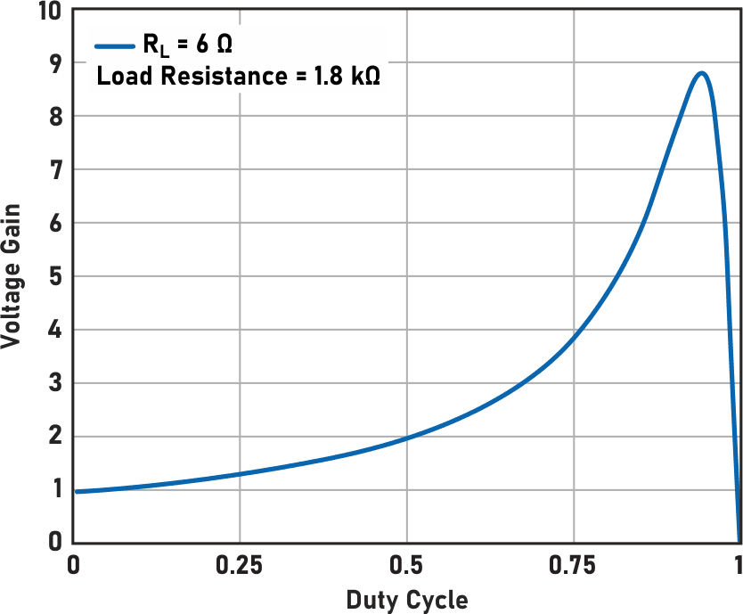 |
|
| Figure 3. | A possible voltage gain when the load resistance is 300 times as high as the DCR of the inductor. |
Figure 3 shows that the maximum voltage gain in this case is only 9. Thus, the conversion of the input voltage of 24 V to 300 V is not possible. The selected DCR, or RL, of the inductor is too high.
In conclusion, the design of a circuit with a boost topology must always include determination of the maximum possible voltage gain. Interestingly, this is dependent on the load resistance – that is, the output current – and the DCR of the inductor. If it turns out that a required voltage gain does not seem possible, a larger inductor with a lower DCR can be selected.