Audio amplifiers for high-power portable speakers such as trolley speakers usually operate with lithium-ion batteries, and these batteries can vary from a single cell to a few cells in series. Designers generally use boost converters to produce the voltage for the audio amplifier, since the speakers may consume more than a few hundred watts.
Because of cost concerns, one approach for high-power audio amplifiers is to use two boost converters in a parallel main-subsidiary configuration, in which the subsidiary converter’s feedback voltage node is grounded and its COMP voltage node is tied to the main converter’s COMP voltage node. Because the COMP node voltage determines the power inductor’s peak current, the subsidiary converter tracks the main converter to produce the same peak current, therefore achieving load sharing between the two converters.
Such an approach is straightforward and effective in peak current balancing. However, it’s the DC current, which is different from the inductor peak current, that determines the actual power. The mismatch in inductor values inevitably results in different DC currents in the two converters, even if their peak currents are identical. Worse, the peak current in the two converters can easily be offset by more than 20%, resulting in a greater current-sharing error from inherent circuit parameter tolerances such as:
- The pulse-width modulation (PWM) controller’s internal offset voltage from the COMP pin to the PWM comparator.
- The current-sense resistor as well as the gain of current-sense amplifier (if applicable).
- The slope compensation signal superimposed on the current-sense signal.
The result is unbalanced power sharing with one converter overheating, a situation that can significantly reduce the system’s overall reliability without a costlier thermal-management scheme.
There are other options, however. This article will discuss simple current-sharing schemes and propose a method to minimize the DC current-sharing error between the parallel boost converters, including experimental results as a proof of concept.
Current-sharing control scheme and operating principle
 |
|
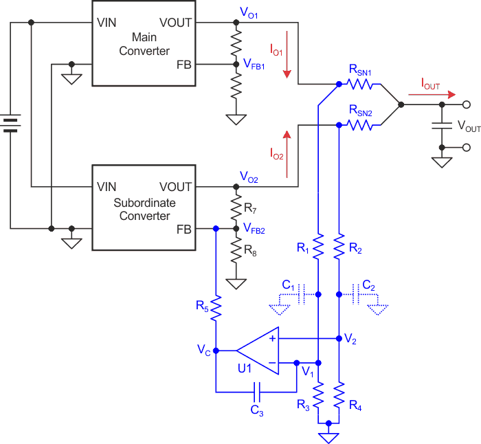
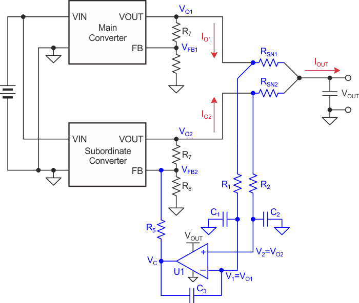
| Figure 1. | In this current sharing control scheme, the subsidiary is forced to deliver the same load current as the main. |
Figure 1 shows a current sharing control scheme in which the subsidiary is forced to deliver the same load current as the main. The sharing control circuit consists of:
- Operational amplifier (op amp) U1
- Current-sense resistors RSN1 and RSN2
- Resistive voltage dividers formed by R1 and R3 and R2 and R4
- Optional sensing filtering capacitors C1 and C2
- Compensation capacitor C3 to stabilize the sharing control loop
- Sharing control resistor R5
Assuming that U1 is an ideal op amp, RSN1 = RSN2, R1 = R2 and R3 = R4. If IO2 becomes greater than IO1 (U1’s output voltage), VC will increase. Consequently, the VFB2 voltage will rise, reducing VO2 and IO2 until IO2 = IO1. Similarly, if IO2 becomes smaller than IO1, the circuit will force VO2 and IO2 to increase in order to reach IO2 = IO1. In short, IO2 will track IO1 in order to achieve balanced current sharing.
In steady state, DC currents IO1, IO2 and IOUT satisfy Equation 1:
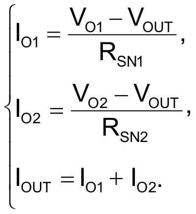 |
(1) |
Analyzing current-balancing errors
In reality, no circuit parameters are perfect. Two factors introduce current-sharing errors to the circuit shown in Figure 1: the tolerances in the resistor values of RSN1, RSN2, R1, R2, R3 and R4, and the input offset voltage and bias currents of U1.
To minimize the current-balancing errors, using the resistors in the E96 series in all six positions – which have 0.1% tolerance – will limit their effects on the sharing error to less than 0.6%.
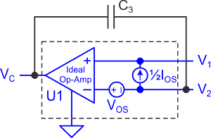 |
|
| Figure 2. | This is how an equivalent circuit of U1 looks like. |
Let’s analyze the errors caused by U1 (see Figure 2). Assuming that the input offset voltage of U1 is VOS, the offset current is IOS, RSN1 = RSN2, R1 = R2 and R3 = R4. After a simple circuit analysis, you can see the sharing error caused by VOS and IOS, as denoted in Equation 2.
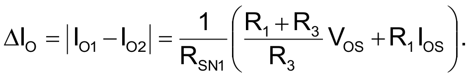 |
(2) |
Equation 2 reveals that:
- An op amp with higher VOS and IOS produces greater errors.
- Higher RSN1 and RSN2 values help reduce the error.
- A higher voltage-step ratio of the resistive voltage dividers leads to bigger errors related to V.
- If R1 = R2 = 0 Ω, the error caused by IOS is eliminated.
There are other constraints in selecting these devices, however. An op amp with ultra-low VOS and IOS is usually expensive. A large current-sense resistor not only causes high power dissipation but also costs more. Therefore, the more cost-effective approach is to optimize the resistor-divider selections.
Optimizing the resistor-divider selections
The resistive voltage divider’s voltage step-down ratio should be as small as possible. In the best case, U1 should be an op amp that can take the converter’s output voltage as the bias supply voltage. That’s because you can then remove the bottom resistor of each divider, as shown in Figure 3. Because of high impedance at the U1’s two input pins, the voltage drop across the top resistor of each divider becomes negligible, enabling U1’s two inputs to have direct sensing of the current difference. The direct sensing minimizes the sensing error and sharing error. It also eliminates the static power dissipation in the resistive voltage dividers.
 |
|
| Figure 3. | An optimal current-sharing scheme shows when VOUT can directly supply U1. |
The switching ripples on the output voltage rails may affect U1’s performance if not attenuated. Employing C1 and C2 to form low-pass filters with R1 and R2 will reduce the ripple voltage at the inputs of U1. Hence, R1 and R2 must not be 0 Ω. You will have to make a trade-off when selecting the values of R1 and R2 and C1 and C2 such that you can achieve the desired ripple attenuation with minimal cost.
Current sharing for parallel boost converters
For some boost converter applications, VOUT may exceed U1’s maximum supply voltage rating. Thus, U1 must have a lower voltage, such as the converter’s bias supply voltage VCC, for its bias supply. In this case, you must use R3 and R4 from Figure 1 to keep V1 and V2 under U1’s bias supply voltage. The drawbacks of doing so are an increased sharing error and associated power dissipation in the resistive voltage dividers.
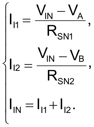
For better performance with parallel boost converters, Figure 4 illustrates a modified current-sharing control scheme. The current-sensing elements are placed on the input side. The operating principle is similar to that of Figure 1, except that this scheme achieves a sharing balance for the input currents of the two converters.
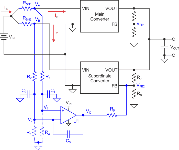 |
|
| Figure 4. | The boost converter current-sharing scheme offers a better performance using a parallel setup. |
Similarly, assuming that U1 is an ideal op amp, RSN1 = RSN2, R1 = R2 and R3 = R4, then the input currents IIN, II1 and II2 satisfy Equation 3.
 |
(3) |
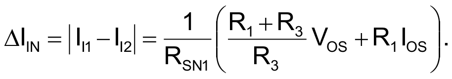
Choosing all six resistors from the E96 series (0.1% tolerance) can limit their effects on the sharing error to <0.6%. The effects of U1’s offset voltage and current are the same as analyzed earlier; namely, Equation 4 calculates the sharing error as follows:
 |
(4) |
Because the input voltage of the boost converter is lower than VOUT, it becomes possible to reduce the required resistive voltage divider’s step-down ratio for a smaller sharing error. If the boost input voltage is smaller than U1’s maximum bias supply voltage rating, U1 can directly take the input voltage, VIN, as its bias supply, and you can remove R3 and R4 to gain the same advantages as discussed earlier.
Experimental results
To prove the concept, let’s employ two LM5155 boost controller evaluation modules alongside the sharing control circuit, as shown in Figure 4. Since the maximum input voltage of the converter is 18 V, selecting the LM8261 op amp for U1 can directly take VIN as the bias supply, thus eliminating R3 and R4. Other selections are:
- RSN1 = RSN2 = 10 mΩ
- R1 = R2 = 499 Ω
- C1 = C2 = 1 µF
- C3 = 100 nF
- R5 = 50 kΩ
According to the LM8261 datasheet, the maximum VOS of U1 is 7 mV, and the maximum IOS is 400 nA. Thus, the worst-case maximum sharing error caused by U1 is 0.72 A, as calculated with Equation 4:
ΔIIN ≤ 1/10 mΩ × (7 mV + 499 Ω × 400 nA) = 720 mA.
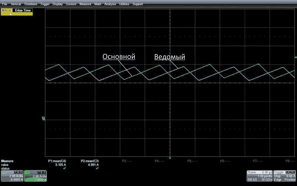
Figure 5 and Figure 6 show two typical experimental results. The input current-sharing errors between the main and subsidiary converters are less than 120 mA, much smaller than the worst-case error of 720 mA.
 |
|
| Figure 5. | The result is shown for input current sharing under VIN = 8 V and a 98-W load. |
The proposed concept was also applied in a reference design of a 9-16 VIN to 50 VOUT, 300-W power supply for typical trolley speakers, which consists of two 150 W LM5155 boost converters in the main and subsidiary configuration.
 |
|
| Figure 6. | The result is shown for input current sharing under VIN = 8 V and a 72-W load. |
Because the input voltage of the boost converter is normally lower than the output voltage, placing the sensing control circuit at the input side helps reduce current-sharing errors. The scheme proposed in this article may be a solution for high step-up-ratio boost converters used in trolley speakers. In such applications, the input is usually a 12-V battery and the output voltage is greater than 40 V, requiring parallel boost converters to support more than 300 W for high-fidelity audio amplifiers, such as the TPA3221. With this scheme, the parallel converter can achieve fairly balanced power sharing.