Cortex-M0+ is not the newest small, low-power processor and, in fact, some newer offerings may surpass it. However, its broad deployment and mature environment continue to make the processor a compelling offering for low-power applications.
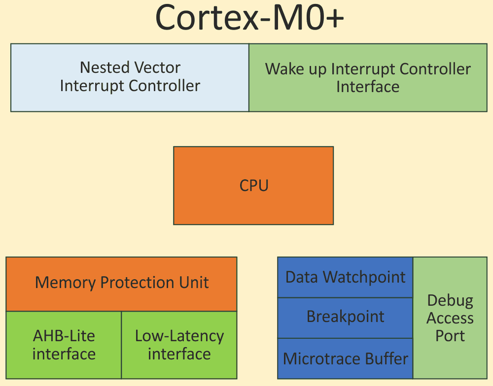
So, what’s important to know about Cortex-M0+ (see Figure 1)? The Cortex-M processor series as a whole is supposed to fill a market need for devices with limited power consumption and are low cost, and thus are suitable for a broad range of applications. The Cortex-M0+ processor takes the family further by offering the smallest footprint and lowest power requirements. This extra step makes Cortext-M0+ a good fit for wearables and sensors.
 |
|
| Figure 1. | The 32-bit Cortex-M0+ is a small footprint microprocessor. |
Cortex-M0+ has been optimized for specific needs, and it includes complete instruction set compatibility with the Cortex-M0. That means identical compiler and debug tools can be used across both.
Cortex-M0+ has a silicon option called Micro Trace Buffer (MTB) that delivers a simple instruction trace buffer. This is in addition to debug capabilities in the Cortex-M0. Cortex-M3 and -M4 features can also be added as silicon.
The key things to know about Cortex-M0+ is that it’s based on ARMv6-M architecture and shares instruction sets with Cortex-M0. The applicable sub-instruction sets are Thumb-1 (most); missing CBZ, CBNZ, IT, and Thumb-2 (some); and only BL, DMB, DSB, ISB, MRS, MSR.
Cortex-M0+ has 32-bit hardware integer multiply with 32-bit results, 1 to 32 interrupts, plus NMI.
The function of the Cortex-M0+ Memory Protection Unit (MPU) is to oversee the CPU's use of memory and make sure no task corrupts the memory or impacts other active tasks. Typically controlled with an RTOS, the MPU can detect attempted memory access that’s not authorized.
Pipelining in Cortex-M0+
Original Cortex-M0 cores (as well as Cortex-M3 and -M4) are built with a three-stage pipeline. Cortex-M0+ is different, relying instead on a two-stage pipeline. Cortex-M0+ lowers power usage and increases performance by reducing pipelining from three to two stages. This higher instructions per cycle relates to branches taking one less cycle. Stage 1 is Fetch & Pre-Decode and Stage 2 is Main Decode & Execute.
Why two-stage? Using a two-stage pipeline rather than three-stage reduces access to flash memory. This is important because flash-memory power needs can often be the primary contributor to power consumption in a microcontroller. Therefore, flash access reduction can significantly reduce overall power consumption.
How many interrupt priority levels does the Cortex-M0+ support?
A nested vector interrupt controller (NVIC), which functions as an interface between the core and any external interrupt sources, is part of the Arm Cortex-M0+. It can support an NMI with properties similar to other external interrupts and connected to the CPU’s NMI request, but separate.
Likewise, an external interrupt controller (EIC) can generate an event and allows for configuration of each interrupt line individually. Pulse and level detection of interrupt signals, low-latency exception handling, and interrupt tail chaining are also supported.
NVIC offers an interface between interrupt sources external to the core (e.g., peripherals and external pins) and the core itself.
Through programming, the priority for each interrupt source is one of four levels. This can be used, for example, when two pending interrupts share the same priority. In such an instance, priority goes to the interrupt with the lowest exception number, otherwise known as the lowest interrupt vector address.
Performance and deployment of Cortex-M0+
Coretex-M0+ is considered one of the most energy-efficient Arm processors for constrained embedded applications. The M0+ has a core pipeline of two stages, which allows it to achieve a power consumption of 11.2 µW/MHz while maintaining a performance of 2.42 CoreMark/MHz. The processor also has three low-power modes that can be used to conserve energy based on processing demands.
According to published sources, the Cortex-M0+ core has been widely implemented across the industry. Examples include:
- ABOV Semiconductor A31G11x, A31G12x, A31G314
- Cypress PSoC 4000S, 4100S, 4100S+, 4100PS, 4700S, FM0+
- Epson S1C31W74, S1C31D01, S1C31D50
- Holtek HT32F52000
- Microchip SAM C2, D0, D1, D2, DA, L2, R2, R3; and PIC32CM JH and MC[31]
- NXP LPC800, LPC11E60, LPC11U60
- NXP (Freescale) Kinetis E, EA, L, M, V1, W0, S32K11x
- Raspberry Pi RP2040 (two M0+ cores)
- Renesas S124, S128, RE, RE01
- Silicon Labs (Energy Micro) EFM32 Zero, Happy
- STMicroelectronics STM32 L0, G0, C0, WL (one Cortex-M4 + one Cortex-M0+) (92)
A number of other devices have Cortex-M0+ as a secondary core. Notably, the small footprint of the Cortex-M0+ core enables it to function successfully as a single core embedded in a larger device as a companion core. In this arrangement, the Cortex-M0+ can provide task partitioning and/or hardware isolation.