Quantum computers are among today’s most exciting emerging technologies, but their design, testing, and manufacturing require unparalleled care to avoid damaging their components. Semiconductors are sensitive, so they require production environments with minimal contamination risks. Cleanrooms are the industry-standard solution, but even these facilities must reach higher standards for quantum computer development.
While a cleanroom overhaul is inherently expensive and disruptive, these costs may be minimal compared to the potential of quantum technology. A quantum chip from Google was recently able to complete a calculation that would take a classic supercomputer roughly 10 septillion years in just five minutes.
This enormous processing upgrade is thanks to quantum computers’ use of qubits instead of bits. Whereas a bit represents either one or zero, a qubit can be both simultaneously – a seemingly small distinction with a dramatic impact on computing speed and power. However, the superconductors and other components necessary to enable this process are highly sensitive to external disturbances.
Many cutting-edge quantum innovations rely on nanotechnology to achieve the desired performance. Nanomaterials have superior thermal stability and electrical conductivity, making them ideal for high-power applications like quantum computing. They also let electronics engineers fit more components in a confined space to uphold Moore’s law.
As helpful as such technologies are, working with them creates an issue in conventional settings. Given their size, nanomaterials are easily contaminateable and breakable. The intensity of quantum operations exacerbates this sensitivity. Even slight deviations in temperatures, light, and air quality could jeopardize the performance of this highly sophisticated and expensive equipment.
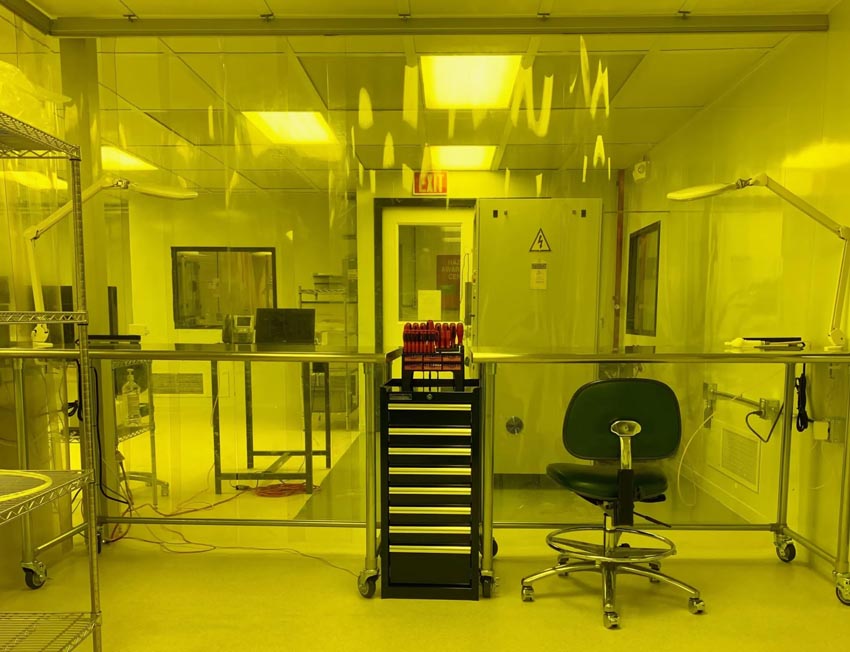
A look inside the quantum cleanroom
Quantum cleanrooms are the solution. Engineers must design and build tomorrow’s cutting-edge devices in equally cutting-edge production facilities. Even a conventional cleanroom may be too prone to contamination and environmental variability to support quantum computer development.
The most common cleanroom ratings [1] today are ISO 7 and 8, which allow concentrations of 352,000 and 3.52 million 0.5-micron particles per cubic meter, respectively. These standards also don’t consider any particulate matter below 0.5 microns. While that’s sufficient for traditional semiconductor engineering, quantum cleanrooms must go further. Ratings of ISO 6 and above that do limit sub-0.5-micron particles are necessary.
Cleanrooms for quantum development also need different sanitation methods. Researchers at Berkeley Lab recently found that gentler component cleaning resulted in an 87% increase in induction [2], making parts more resistant to electrical noise. The method in question used lower temperatures, vacuums, and suspended components to minimize environmental hazards.
Even lighting and ambient temperatures require attention in the quantum cleanroom. Many of these components are photosensitive to blue wavelengths, particularly, so overhead lights should lean more toward the warm end of the spectrum. Quantum circuits also tend to be temperature-sensitive, so these cleanrooms must use gentle refrigeration techniques to keep the area cold.
Quantum electronics engineers must get used to cleanrooms
As quantum technology advances, electronics design engineers may need to adapt to it. The professionals designing, testing, and producing tomorrow’s most advanced electronics must learn to work with their unique production requirements. Getting used to the quantum cleanroom is a crucial step in getting ready for this next generation of computing.