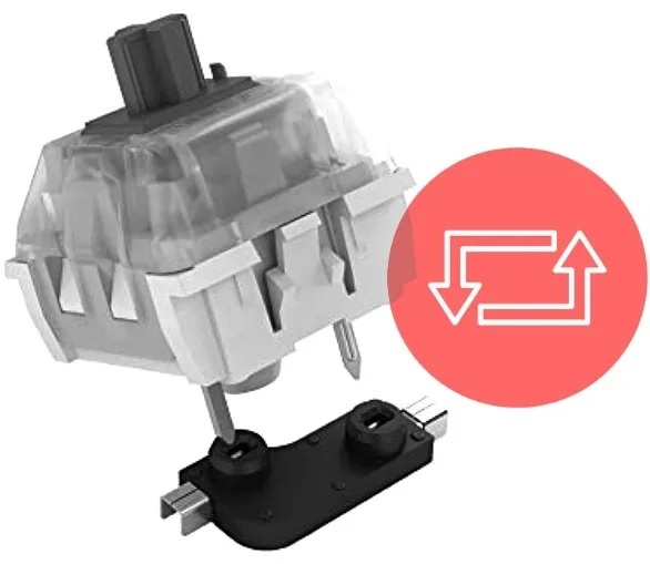
Most mission-critical systems need to be designed for near-zero downtime throughout their useful life. So, if a component of such a system fails or needs updating, it must be replaced without interrupting the rest of the system. Here, the board or module will have to be taken out, and its replacement plugged in, while the system remains up and running (Figure 1).
 |
|
| Figure 1. | In hot swapping, a circuit is taken out and its replacement is plugged in. |
This process is known as hot swapping (hot plugging).
Next, a hot swap controller is a dedicated device or integrated circuit that manages the insertion and removal of circuit boards (or components) from a live system without interrupting the operation of the system or causing damage.
In essence, the hot swap controller circuit, wired between the board input power supply rail and the rest of the board’s circuitry, is an inrush current limiter that allows for charging of the bulk capacitance in a controlled manner. Besides, certain faults such as over-current and over-voltage are handled by the hot swap controller circuit.
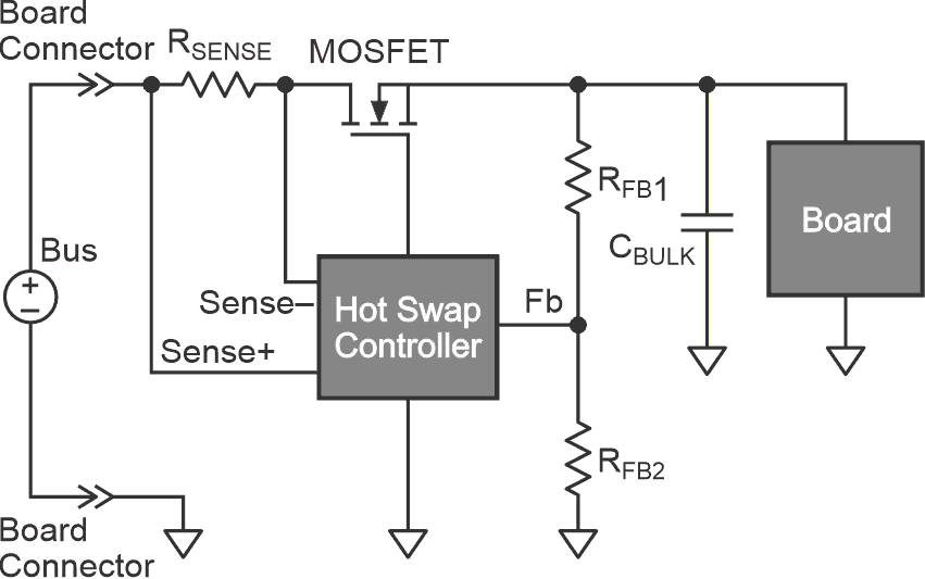
Here is how a generic hot swap implementation looks like (Figure 2).
 |
|
| Figure 2. | Here is a closer look at an arrangement built around a hot swap controller. |
When the board is connected to the bus, the capacitor CBULK will charge with a large inrush current if the hot swap controller is not present. With the hot swap controller in place, the inrush current is sensed via voltage drop across the current sense resistor RSENSE, and it is then used to limit the current. The feedback Fb pin is used to monitor the output voltage for under- and over-voltage conditions. A critical component in this setup is the power MOSFET.
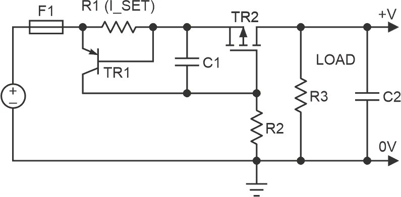
This circuit idea for hot swap applications uses a regular PNP transistor (TR1) and a current sense/set resistor (R1) to provide continuous current sensing and limiting (Figure 3). As power is applied, current flows through R1 and TR2 to the LOAD. Current through R1 creates the VBE bias voltage for TR1. If the current is large enough to bias TR1 on, then TR1 limits conduction through TR2 to the LOAD by scaling down the gate-source voltage of TR2.
 |
|
| Figure 3. | Here is how a typical discrete hot swap topology looks like. |
The biggest challenge that a design faces with any hot swap controller is selection of the correct MOSFET used as a pass element. This is because while charging bulk capacitor, the MOSFET will be in the linear region, thus risking an overheating failure due to fast joule heating.
This means that the MOSFET is operated in the linear regime during the pre-charge phase, with a large voltage across it until the bulk capacitor (load capacitor) is fully charged, at which point the MOSFET reaches its fully-on state and runs with its stated RDS-ON resistance. So, the entire pre-charging energy is dissipated in the MOSFET, and it becomes very stressed. Note that the capability to handle the current charging is related to the MOSFET’s safe operating area (SOA), and this capability depends on the die and package size.
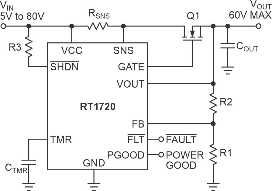
Notably an IC-based hot swap scheme offers many features in a small package and the IC necessitates only a few external components. Figure 4, for example, depicts the simplified application circuit of the RT1720 hot swap controller with fault timer.
 |
|
| Figure 4. | The application is built around the RT1720 hot swap controller. |
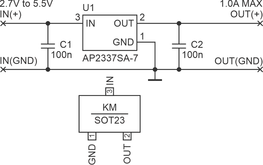
For some quick experiments related to this post, I randomly selected the AP2337 hot swap controller IC.
The AP2337 is a single-channel current-limited integrated high-side power switch optimized for hot swap applications. The device, available in SOT23 package, offers reverse current blocking, over-current, over-temperature and short-circuit protection, as well as controlled rise time and under-voltage lockout functionality.
The AP2337 application circuit is shown in Figure 5.
 |
|
| Figure 5. | AP2337 offers a fast short-circuit response time to improve overall system robustness. |
Since this was just a quick experiment and I was driving a simple test load, I deliberately took some temporary shortcuts. When I do something more with this concept, I will solder everything to a perf board or a custom PCB to make it more robust.
To sum up, hot swapping, at a minimum, demands that you limit inrush current to prevent the possibility of a system wide brownout when a large capacitive load is energized. The hot swap controller is a crucial element in a critical control system, where continuous operation is essential, permitting the replacement of faulty modules and/or components without system interruption.