Bob Zwicker, Analog Devices
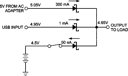
Many systems must select among two or more low-voltage dc-input sources, such as an ac adapter, a USB (Universal Serial Bus) port, or an onboard battery, for example. You can implement this selection using manual switches, but automatic switching is preferable. You usually want to use the highest-available input voltage to power your system. You can accomplish this task using a Schottky-diode ORing scheme (Figure 1). Unfortunately, the forward-voltage drop of a Schottky diode ranges from 300 to 600 mV. This voltage wastes power, creates heat, and decreases the voltage available to your system.
 |
|
| Figure 1. | Schottky-diode ORing can power a load from the highest input-voltage source. |
Efficient voltage ORing requires only a P- or an N-channel MOSFET, a suitable op amp, and a few passives. This Design Idea describes the application of voltage ORing to positive dc-power rails. The P-channel-MOSFET design is suitable for low-power, single-supply systems operating at 3.3V or higher, and the N-channel MOSFET fits situations in which the bus voltage is lower or the current is higher and a suitable op-amp bias voltage is available.
Positive current flows from the MOSFET drain in an N-channel-FET design. In a P-channel design, the current flows from the MOSFET source. The MOSFET’s drain-body diode would defeat rectifier operation if the usual current flow (for switching or amplification) were used.
Your first design task is to choose a suitable MOSFET. The MOSFET’s worst-case on-resistance must be low enough so that the I×R (current-times-resistance) drop with full-load current is low enough to accomplish the design objectives. A 0.01Ω MOSFET has a 50-mV forward-voltage drop when 5A flows through it. Be sure to consider power dissipation due to R×I2 and the resulting temperature rise.
Your second design task is to choose an op amp. The op amp must be able to operate with the voltages involved and to adequately drive the MOSFET’s gate voltage. The P-channel design requires a rail-to-rail I/O type. A single-supply op amp is adequate for the N-channel design. Another important consideration is the op amp’s input offset voltage, VOS. The total ±VOS window must be less than the maximum desired voltage drop across the MOSFET. For example, if you permit a 10-mV forward-voltage drop at full load, then the op amp should specify an offset voltage of ±5 mV or better.
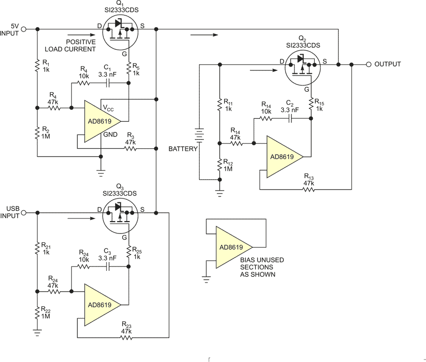
R1/R2, R11/R12, and R21/R22 form the input-voltage divider, which biases the op-amp input at a level slightly below that of the input voltage that it is controlling (figures 2 and 3). This offset must exceed the op amp’s maximum offset voltage to ensure that all op-amp parts in production always turn off the MOSFET when you apply reverse voltage. In the example of the P-channel 5V design, R1 and R2 bias the inverting op-amp input at 99.9% of the input voltage, or 4.995V dc. In steady-state operation, the op amp servos with the conducting MOSFET to keep the other op amp’s input at the same voltage, within the tolerance of the op amp’s offset voltage. With a perfect 0V-offset op amp, light-load currents cause the MOSFET to only partially enhance, so the circuit delivers a 5-mV MOSFET forward-rectifier drop. This mild effect is the only disadvantage of R1 and R2’s input offset biasing. If the MOSFET resistance is too high to allow it to maintain 5 mV at full load, then the op amp fully enhances the MOSFET as its output swings to the rail, and the ORing circuit delivers the MOSFET’s fully enhanced on-resistance.
 Click to enlarge |
|
| Figure 2. | MOSFET power ORing using P-channel MOSFETs is the more common choice for single-rail systems when the rail voltage is sufficient to operate the op amp and drive the MOSFET gate. |
 Click to enlarge |
|
| Figure 3. | MOSFET power ORing using n-channel MOSFETs is more suitable for low-voltage rails or for high current when a suitable op-amp bias supply is available. |
You can consider the MOSFET’s variable on-resistance as the element with which the op amp senses current. When you apply reverse voltage, the MOSFET de-enhances, the I×R voltage drop increases, and the op amp’s output ends up at the appropriate supply rail, driving off the MOSFET as hard as it can.
With light-load conditions and a given offset voltage, the op amp tries to servo the voltage on its power-output-sensing input to the voltage on its power-input-sensing input plus the offset voltage. With R2 open-circuited, the op amp has no intentional external offset. If the op amp’s offset voltage were in the unfavorable direction, a sizable reverse-cutoff current would occur if the input-power bus were to fall to a lower potential than the output-voltage bus.
Figure 4 shows current-voltage test data for the operating region. The complete design, including intentional offset, produces the green curve. The equivalent of an unfavorable internal offset and no intentional external offset produces the blue curve. Although the green curve sacrifices some forward-voltage drop at light-load conditions, its forward voltage is always less than the full-load maximum. The intentional offset avoids any significant reverse current in the MOSFET. This design can switch at the 0A current transition, at which the leakage-current MOSFET’s drain-body diode is likely to dominate.
 |
|
| Figure 4. | The green curve shows results with the correct external offset applied. The blue curve shows results when the op amp's internal offset is in the unfavorable direction and no external offset is applied. |
On the other hand, the blue curve, without intentional offset, permits significant reverse current under some circumstances. This example shows approximately 100-mA reverse current with 2-mV reverse voltage across the MOSFET before the circuit switches off the MOSFET. Both the P- and the N-channel designs have undergone testing, and the P-channel design is in production.