Because they use practically no bias current (a useful feature in itself), JFETs also have practically no current noise. This feature means that you can use JFETs in very-high-resistance circuits and obtain good noise performance. JFETs are also fast devices, with garden-variety types specified in the hundreds of megahertz. On the flip side, JFETs are difficult to exploit in a manufacturing environment because they have widely varying dc specifications. With a simple resistor-based bias network, the same part number can give results that differ by several volts from device to device. One way to use JFETs in a repeatable and manufacturable manner is to use the topology that Figure 1 shows. The purpose of the op amp is to bias the JFET at VGS = 0 V and, therefore, at ID = IDSS. It meets this goal by increasing the current in the bipolar transistor until VGS = 0 V and ID = IDSS.
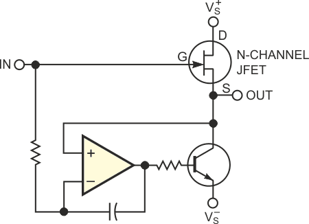 |
| Figure 1. |
The op amp biases the JFET at IDSS, with VGS = 0 V. |
In this condition, the JFET operates at its highest gain (gm) and lowest voltage-noise condition. The JFET operates as a follower with zero offset. The only requirement for the op amp is that it have ultralow bias current. A variety of op-amp types satisfy this criterion, including JFET-input op amps, such as the LT1462; superbeta-input op amps, such as the LT1097; and micropower op amps, such as the LT1494. Figure 2 shows an implementation of the topology of Figure 1, using an inexpensive, fast 2N5486 JFET. This device specifies IDSS at 8 to 20 mA at room temperature. The LT1097 maintains the gate-source voltage at 0 V by adjusting the JFET's drain current. The source of the JFET connects to the inverting input of the 325-MHz, low-noise LT1806 op amp. RF closes the loop back to the JFET's gate. In this application, the circuit serves as a transimpedance amplifier for a fast photodiode.
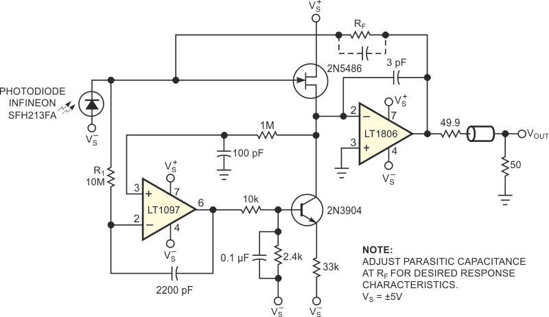 |
| Figure 2. |
This fast, high-gain photodiode amplifier uses Figure 1’s scheme to bias the JFET. |
Selecting a high value, 10 MΩ for R1 maintains low noise gain, but you could reasonably reduce it to a few times larger than RF. The values of the other resistors and capacitors in the LT1097 loop to attenuate the noise and shape the noise bandwidth of the slow loop. Measurements show the output-noise spectral density is 9 nV/ÖHz with RF = 0 Ω, so resistor noise dominates with RF greater than approximately 10 kΩ. Table 1 shows the rise time and bandwidth achieved for several transimpedance gains (as set by RF). To obtain optimum speed characteristics, you make ’parasitic-capacitance adjustments' (the capacitor with broken lines in Figure 2) by adjusting the proximity of RF’s leads to its body. Figure 3 shows the time-domain pulse response with RF = 1 MΩ. Connecting two 499-kΩ resistors in series improves the response.
| Table 1. |
Results for various RF with 1.2 V output step |
| RF |
10 to 90% rise time
(nsec) |
3-dB bandwidth
(MHz) |
| 100 kΩ |
64 |
6.8 |
| 200 kΩ |
94 |
4.6 |
| 499 kΩ |
154 |
3 |
| 1 MΩ |
263 |
1.8 |
|
| |
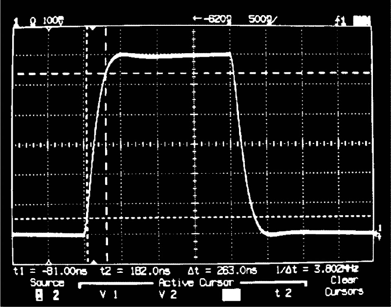 |
| Figure 3. |
The circuit of Figure 2 exhibits clean pulse response with little
overshoot or ringing. |
Materials on the topic
- Datasheet Analog Devices LT1097
- Datasheet Linear Technology LT1806
- Datasheet ON Semiconductor 2N5486
- Datasheet OSRAM SFH213 FA