This automatic pulse generator (figures 1 and 2) is a test gadget that senses a probed contact to a pair of terminals under test and automatically issues a momentary power pulse to them once proper contact is made. These terminals could be the input of a logic gate, an LED on a circuit board, a transformer or relay coil, etc. The need for such a pulse often arises in the day-to-day engineering work of experimenting and testing.
 |
|
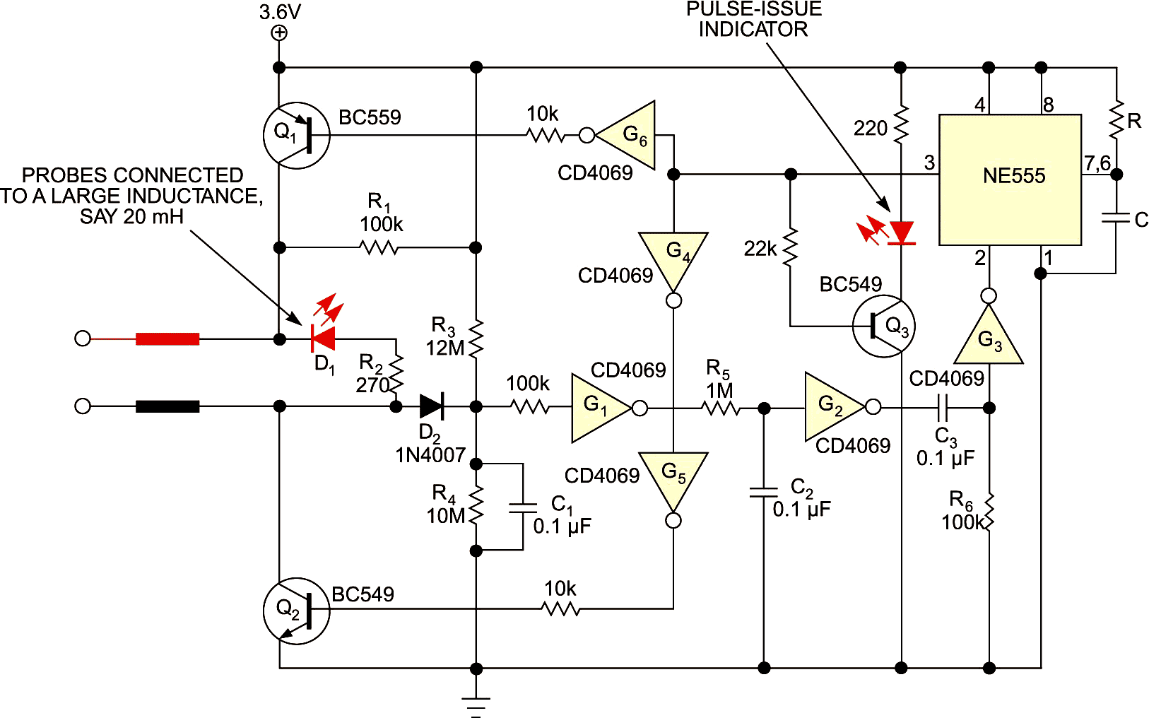
| Figure 1. | The NE555 version is easy to get working but has an increased parts count. |
 |
|
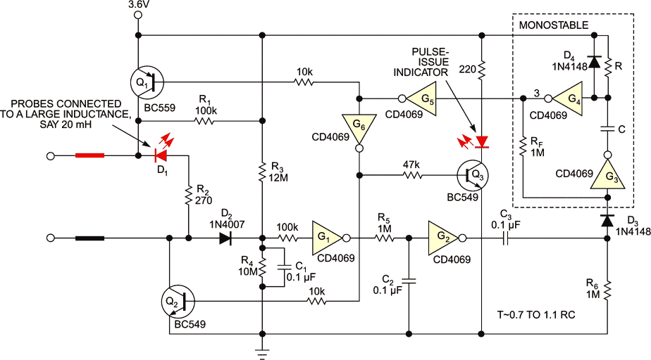
| Figure 2. | You can eliminate the NE555, but variations in the G4 input switching threshold can affect the pulse duration. |
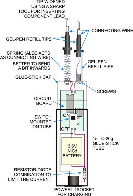
The gadget is powered with a small 3.6V rechargeable NiCd battery. You can easily construct it in a glue-stick tube (Figure 3) with the special arrangement of probes shown. A regular arrangement of independent probes also may be used. The circuit has been tested with a 5V supply, as well.
 |
|
| Figure 3. | You can build the automatic pulse generator in a used glue-stick tube. |
Two versions are shown: Figure 1 uses an NE555 timer IC as a monostable and is the easiest to get working. Figure 2 eliminates the NE555 for a reduced parts count but could be affected by variations in the parameters and different manufacturers of the CD4069 CMOS hex inverter used in place of the NE555.
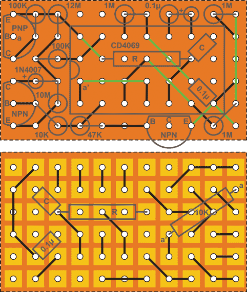
The single chip version of the pulse generator can be built on a small piece of 6×11 GCB (general purpose circuit board), which can be easily accommodated into the glue stick tube (Figure 4).
 |
|
| Figure 4. | The pulse generator prototype on perfboard. |
Transistors Q1 and Q2 are switches that connect the +ve and −ve probes to the 3.6V supply and ground when turned on by the CD4069 and the NE555. R3 and R4 bias gate G1’s input just below the switching threshold to hold its output high, which holds the output of gate G2 low. The time constant formed by C1 provides a certain amount of noise immunity and determines the minimum time for which the test circuit should be connected between the probes. The 100-kΩ resistor in series with the input of G1 limits the input current in case the probe is accidentally connected to an active circuit.
R1 connects to the junction of R3 and R4 through a reverse-biased diode, D1. It normally has no effect as long as the probes are not connected through a load, because the series string of R1, D1, R2, and D2 is a high-resistance circuit compared with the 12 MΩ of R3. As soon as you connect a passive test circuit such as a resistor/inductor/LED, however, D1 and R2 are paralleled by it. Thus, the branch in parallel with R3 has a lower resistance and the G1 input voltage increases such that it is now recognized as logic 1, driving G1’s output low.
R5 and C2 form a debounce-and-delay network to ensure that the probes are firmly connected to the circuit under test before the power pulse is issued. When the output of G1 goes low, capacitor C2 begins to discharge through R5. The logic input voltage of G2 changes within a time on the order of R5C2.
In Figure 1, the rising output of G2 immediately triggers the NE555 monostable through G3 and the differentiator formed by C3 and R6. Once C3 has finished charging through R6, G3’s input returns to ground and its output returns high to allow the NE555 to complete its timing cycle with a duration that its R and C values determine.1 The timed logic 1 output of the NE555 turns on Q3 to light the “pulse issued” LED, and through G4, G5, and G6 turns on Q1 and Q2 to present the power pulse to the circuit under test.
Only one pulse is generated per contact; removing the probes and then reconnecting them will issue a new pulse. If the circuit under test is inductive and greater than 20 mH at the end of the pulse, the inductive back EMF will flash LED D1 if the probes are still connected.
In Figure 2, the NE555 has been replaced by a monostable comprising G3 and G4, D4, and RF. R6 has been changed to 1 MΩ, and diode D3 has been added to the input of G3. Resistor R holds G4’s input high, which in the quiescent state causes G4’s output to hold G3’s input low. A rising edge from G2 causes a low to couple through the initially discharged capacitor, C, to G4, whose rising output is fed back to G3 as positive feedback and holds G3’s input high even if the probes are removed. If this happens, D3 becomes reverse biased and prevents G2’s falling edge from affecting the monostable operation.
Capacitor C then slowly charges through resistor R until G4’s input rises above its switching threshold, and the positive-feedback process reverses. The pulse duration depends on the R×C time constant, and is about 0.7 to 1.1 RC, depending on the G4 threshold voltage, which can vary between 0.33 and 0.67 of the supply voltage. The author suggests 1 MΩ for R and 40 nF for C, but R could be made variable, as well. D4 ensures that C discharges rapidly as G3’s output returns high.
In either case of Figure 1 or Figure 2, the momentary high output of the monostable turns Q3 on to flash the pulse-issued indicator LED. It also turns on both Q1 and Q2 to power the probes. D2 serves to isolate the −ve probe from the primary input of the circuit at G1 to avoid immediate self-suppression.