This circuit solves the problem of sending data over a cable with no free conductors. The data is OOK (on-off keying) modulated and superimposed on a high-frequency carrier so it can be sent over a low-voltage power supply line.
Sometimes a circuit requires a data link over an existing cable that doesn’t have any free conductors for a dedicated comm link. A common solution is to superimpose a high-frequency carrier modulated by the data onto a power-supply line, particularly over high-voltage household wiring.
However, a Web search reveals that although many designers face this problem, no simple, inexpensive, and reliable solution for low-voltage systems has been widely publicized. This idea describes such a low-voltage solution. (Note that the circuit is not suitable for high-voltage applications unless specific measures are taken to ensure safe operation.)
The circuit, which requires only a handful of discrete components and two ICs, can reliably transfer data at rates up to at least 32 kbits/s with a 2.6-MHz carrier and probably well beyond that if a higher carrier frequency is used and component values are adjusted accordingly. The link can tolerate cable capacitance of up to 10 nF and has low radiated emissions. The circuit transmits data in standard (UART-compatible) asynchronous serial format, but designers can use Manchester encoding or other protocols.
For simplicity’s sake, the modulation scheme is on-off keying (OOK), and the circuit provides no inherent noise rejection (other than a good signal-to-noise ratio). Designers can implement error detection/correction in software if desired.
 |
|
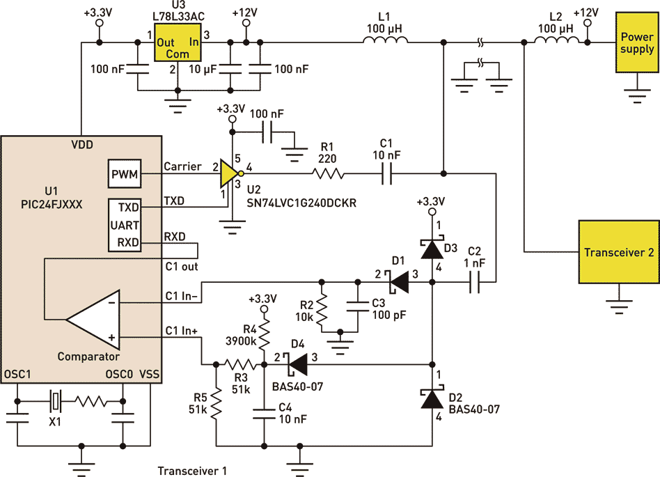
| Figure 1. | A relatively simple circuit allows users to communicate data over a low-voltage power line in applications that do not have any free conductors in an existing cable. |
U1 is a PIC microcontroller that includes several peripherals ideally suited for this application, in particular a pulse-width modulation (PWM) module or programmable time base for generating a square-wave carrier and a high-speed analog comparator whose input common-mode range includes ground or very close to ground (Fig. 1). Other MCUs with similar peripherals will probably work as well.
The circuit is a two-transceiver system. Transceiver 1, on the left, is a “remote” node getting its power from the “base” unit, Transceiver 2, on the right. Inductors L1 and L2 isolate the high-frequency carrier from the low impedances on the power sides of the bus.
Multi-drop configurations are possible as long as each node includes an inductor to maintain the high impedance of the data-carrying portion of the power line. The inductors can be small surface-mount devices, as long as their current ratings, with a generous margin, are sufficient for the load(s).
The transmitter portion of the transceiver comprises a TinyLogic tri-state line driver, U2, whose output is coupled to the bus by R1 and C1. R1 provides a bit of filtering to minimize electromagnetic interference (EMI) from the sharp edges of the square-wave carrier.
The receiver comprises a clamp formed by C2, D2, and D3, followed by two peak detectors. The first, with a time constant of approximately one-third of the data bit time, demodulates the carrier to recover the data timing. The other, with a time constant of about 50 times the bit time, adaptively follows the carrier level. R3 and R5 divide this level to approximately two-thirds of the carrier amplitude.
The demodulator and reference level outputs are applied to the inputs of the MCU’s internal analog comparator to square up the final data, which is then routed externally to the MCU’s UART. Resistor R4 biases the positive input of the comparator slightly positive to ensure a predictable logic-high idle state.
It should be noted that since the transceiver’s input and output are always connected, the software must ignore reception of its own transmissions.
 |
|
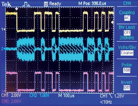
| Figure 2. | The original data (yellow) is transmitted over the power line on a modulated carrier (blue) and faithfully recovered at the comparator’s output (pink). |
In Figure 2, trace one (yellow) is the original digital data sent from a remote transceiver’s UART TX port. Trace 2 (blue) is the resulting modulated carrier present on the power line. Trace 3 (pink) is the demodulated and reconstructed data presented by the receiver’s comparator to its UART RXD port.
 |
|
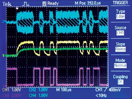
| Figure 3. | This screen shows the demodulation and reconstruction process with the modulated signal (blue), the negative comparator input (yellow) and the positive comparator input (green), and the reconstructed data (pink). |
Figure 3 depicts the demodulation and reconstruction process. Trace 2 (blue) is the incoming OOK-modulated carrier, and the comparator inverting and non-inverting inputs are shown on traces 1 (yellow) and 4 (green), respectively. The comparator’s output, which is the reconstructed data presented to the UART’s RXD, is shown on trace 3 (pink).