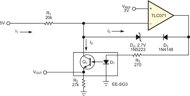
The transfer gain of optical sensors spans a 16-to-1 ratio because of variations in the LED, phototransistor, ambient temperature, and optical path. The wide transfer-gain variation complicates output-resistor selection in dc-coupled circuits. You must size the output resistor to prevent high transfer gains from causing output-stage saturation, but low transfer gains yield low output-voltage swings with low-value resistors. You usually need to make adjustments to match the dc output voltage to the transfer gain, and reliable operation requires readjustment under extreme temperature and dust conditions. The circuit in Figure 1 eliminates the need for adjustments. The circuit uses dc-coupled feedback to control the current in the output resistor. Hence, the output voltage is predictable and constant.
 |
||
| Figure 1. | The op-amp feedback keeps the phototransistor’s current constant, so the circuit requires no adjustments for transfer gain. |
|
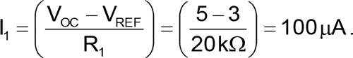
The op amp's input current and the current in D3 is negligible, so I1 = I2, and the output voltage is 2.7 V when the phototransistor is on (light path unbroken). The output voltage is 0 V when the phototransistor is off (light path broken). The op amp's output-voltage swing accommodates the variation in transfer gain. This output voltage assumes the value required to make the LED current times the transfer gain equal to the phototransistor's emitter current. The input-current equation is as follows:
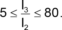
The range of transfer gain is 80 to 5:
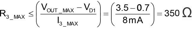
The op amp's output-voltage range is limited, especially with the high output-current requirement, thus the design uses a TLC071 that can source 20 mA at 3.5 V in this design:
When the light is blocked, the phototransistor's emitter current goes to zero. The input current, I1, can't flow into Q1 because it is off, so the op amp heads for the positive rail. If the op amp's output stage saturates, the recovery time is unpredictable, so you insert the zener-diode combination D2 and D3 to prevent saturation. As the op amp's output voltage approaches 3.4 V (VD2 + VD3), the diodes clamp the output voltage, thus preventing saturation. R3 = 270 Ω so that it can supply adequate LED current without incurring op-amp saturation. When this circuit drives a saturated logic circuit, you should buffer the output with a hysteresis gate or a comparator with hysteresis.