AC signals can emanate from many sources, and many of these sources are incompatible with the most popular interface voltages, such as TTL. A temptation always exists to capacitively couple the ac signals because capacitive coupling strips off the dc level. Capacitive coupling sometimes doesn't work, because the coupled signal's voltage swings around ground, so you have to add dc offset to make the coupled signal compatible with the interface voltage. Also, the coupled signal contains a dc content, VDC, which varies with pulse width, and the dc variation interferes with the interface voltage when the signal swing is large.
 |
|
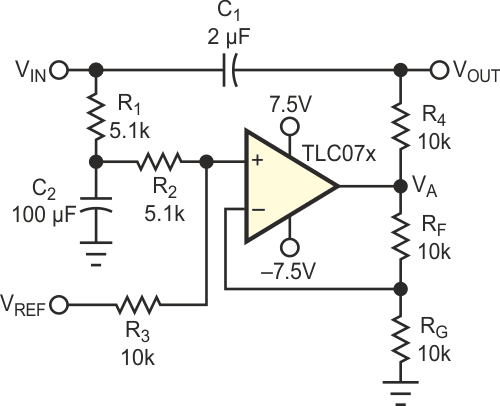
| Figure 1. | This circuit is a universal level shifter for ac signals; it accommodates any interface standard. |
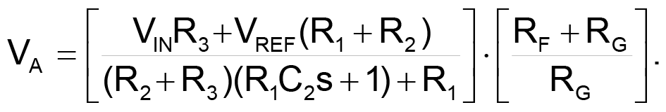
This circuit completes the signal interface by measuring the dc offset, adding appropriate compensation to the capacitively coupled signal and adding an adjustable-dc- level feature (Figure 1). R1 and C2 form a lowpass filter (f3dB = 0.312 Hz) that measures the dc content of the input signal. The transfer equation is the following:
When R1 + R2 = R3 and RF = RG, VDC transfers to the output signal, VA, because it is multiplied by ½(2) = 1 or a gain of one. The output voltage for the same resistor values contains VREF; thus, the output signal is level-shifted by the voltage, VREF, not VREF plus the VDC. When the input signal's duty cycle changes, rather than the output voltage's changing with duty cycle, the op amp keeps the output-voltage level constant.
The gain for the VDC must be one, so that it cancels the voltage shift after ac-coupling. The gain for the reference voltage can be greater than one; for example if R1 + R2 = 3R3 and RF = 3RG, the dc content is ¼(4) = 1, and the reference-voltage gain is ¾(4) = 3. VREF can be positive or negative, so you can obtain TTL, CMOS, or ECL logic levels with this circuit. The time constant formed by C1 and R4 must be large enough to pass the lowest frequency signal without distortion. The value of R4 is not critical, as long as the op amp can drive R4 without losing too much signal swing. In some cases, you can size R4 to present the driving-point impedance you need to eliminate near-end reflections. The circuit easily couples 400-MHz data as configured, but the data rate depends on the time constant formed by R4 and the input impedance of the driven circuit.