Introduction
Positive to negative conversion (inverting output) is widely used in LCD devices, OLED displays, audio amplifiers, industrial machinery, semiconductor manufacturing process control equipment, measurement tools, testing systems, LED drivers and battery chargers. Many of these applications require high power levels and extended input voltage ranges, two inherent features of the LTC3896 positive to negative controller. This controller is especially well suited for automotive applications due to its ability to handle very high input and output voltages (total voltage stress can reach 150 V), its ability to drive standard level MOSFETs and its low operating quiescent current 40 μA (10 μA in shutdown).
Wide 7 V to 72 V Input to −12 V at 5 A Output
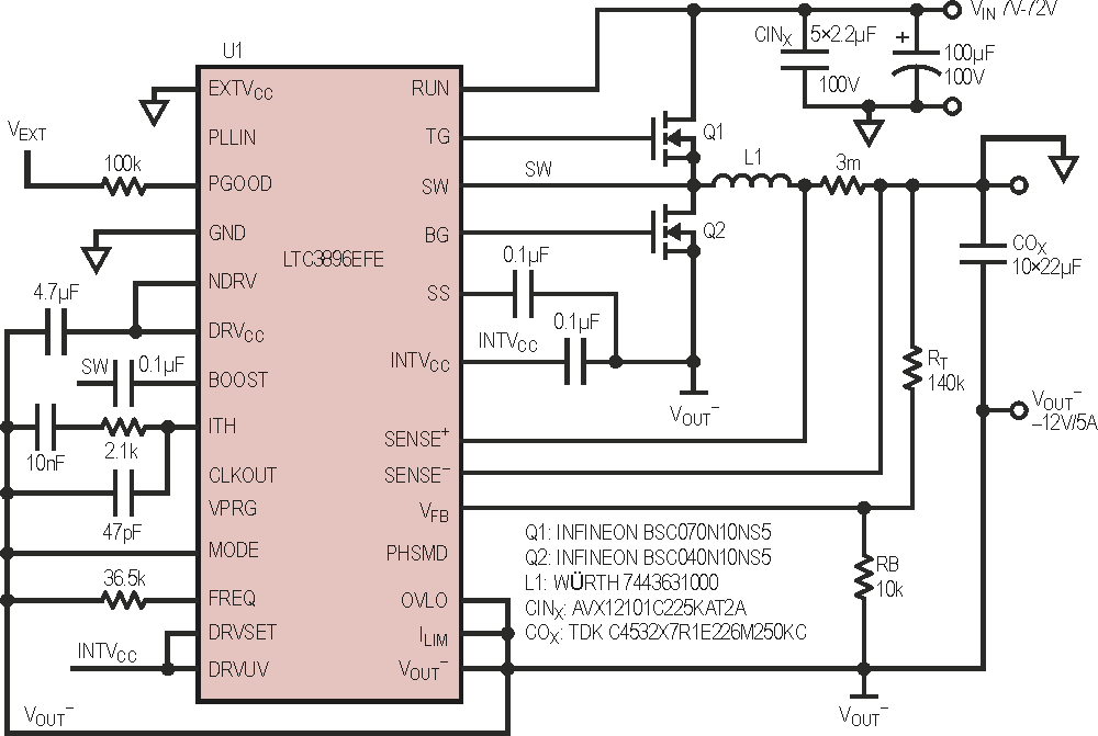
Figure 1 shows a positive to negative converter based on the LTC3896. This solution delivers −12 V at 5 A from a 7 V to 72 V input voltage range. In the automotive market, the LTC3896’s ability to handle high input voltages eliminates the need for bulky and costly voltage suppressors, while the low minimum input voltage keeps sensitive systems operational even during cold crank conditions.
 |
||
| Figure 1. | The –12 V Output Converter (U1) Provides 5 A to the Load in the Input Voltage Range from 7 V to 72 V. Note Control Signals RUN, PGOOD and PLLIN are Referenced to GND. |
|
The power train of the converter comprises MOSFETs Q1, Q2 and inductor L1. The output filter is based on ceramic capacitors COX. The EXTVCC pin of U1 is connected to GND, producing a 12 V potential at this pin relative to VOUT–. If a power good signal is required, an external voltage source referenced to GND should be employed. The LTC3896’s control and interface signals, including RUN, PGOOD and PLLIN are referenced to the system GND to eliminate the need for level shifters in processor controlled systems.
The guidelines for calculating voltage and current stress on the components surrounding the LTC3896 are detailed in the data sheet. For a basic evaluation, duty cycle (D), average inductor current (IL) and MOSFET voltage stress (VDS) can be calculated by the following:
Demonstration Circuit DC2447A [1] illustrates the versatility of the LTC3896. Designers can test the numerous functions of this controller, including synchronization to an external clock, the ability to employ an external linear regulator to reduce thermal stress on the IC at high output voltages and easy solutions for generating –5 V or –3.3 V outputs.
 |
||
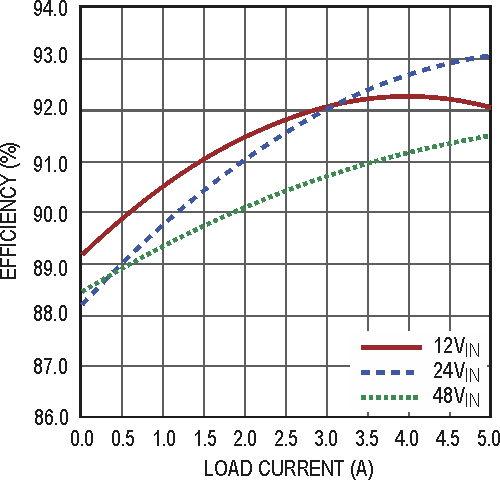
| Figure 2. | Efficiency Curves for the Circuit in Figure 1. Output Voltage is –12 V and Maximum Load Current is 5 A. |
|
Figure 2 shows efficiency at various input voltages. Figure 3 shows a thermal image of the converter in action.
 |
||
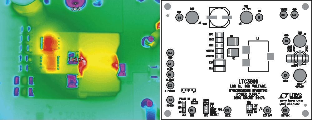
| Figure 3. | Thermal Image of DC2447A is Taken at 36 V Input Voltage, –12 V at 5 A Output. On the Right Side, an Assembly Drawing of the Demo Board. |
|
Conclusion
The LTC3896 is a highly integrated controller, specially designed for positive to negative conversion. Solutions based on this controller are highly efficient, with extremely low quiescent current – important for battery-operated systems. It is also highly versatile, featuring programmable frequency, a wide 150 V input voltage range and output voltages to –60 V. It simplifies the design of automotive and industrial supplies with control signals referenced to host ground.