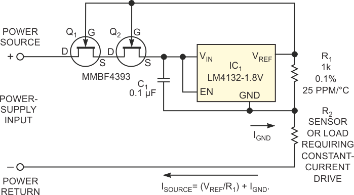
Many process-control sensors, such as thermistors and strain-gauge bridges, require accurate bias currents. By adding a single current-setting resistor, R1, you can configure voltage-reference circuit IC1 to produce a constant and accurate current source (Figure 1). However, the source's errors depend on the accuracy of both R1 and IC1 and affect measurement accuracy and resolution. Although you can specify high-precision resistors whose accuracy exceeds that of most commonly available voltage-reference ICs, the voltage reference's error dominates this current source's accuracy. Although the manufacturer minimizes the voltage reference's temperature sensitivity and output-voltage error, sensitivity to power-supply variations can affect its accuracy, especially in process-control applications that must operate over a wide range of supply voltages.
 |
||
| Figure 1. | A pair of cascode-connected JFETs reduces the effects of power- supply-voltage fluctuations on a current source’s accuracy. |
|
A cascode-connected pair of JFETs, Q1 and Q2, form a constant-current source that minimizes the reference circuit's sensitivity to supply-voltage fluctuations and extends IC1's operating voltage beyond its 5.5 V maximum rating. In addition, Q1 and Q2 effectively increase the current source's equivalent resistance from a few megohms almost into the gigohm range. In the circuit's Norton model, equivalent resistance represents the parallel resistance across an ideal current source.
An N-channel JFET operates as a depletion-mode device at its maximum saturated drain current when its gate-to-source bias voltage is 0 V. In contrast to a depletion-mode MOSFET that requires a gate-bias voltage to conduct, the JFET operates in a default on-state and requires gate-bias voltage to cut off conduction. As its gate-to-source voltage becomes more negative with respect to the source, a JFET's drain current goes to zero at the pinch-off voltage. The JFET's drain current varies approximately with its gate bias:
where ID is drain current, IDSS is the saturated drain current, VGS is the gate-to-source voltage, and VP is the pinch-off voltage.
Assume that IC1's output voltage, VREF, remains constant at 1.8 V. Because the output voltage drives Q2's gate, IC1's input voltage, VIN, equals

Thus, Q2's gate-to-source voltage rests at its nominal pinch-off voltage of 1.2 V and varies in step with small changes in current source. As the power-supply voltage varies from 3 V to more than 30 V, then the input voltage remains almost constant, as you would expect, because VREF also remains constant. The cascoded-FET configuration increases the current source's Norton equivalent resistance beyond that of the voltage reference and R1 alone. You can use a single JFET, but stacking two JFETs further enhances the circuit's effective impedance. Note that IC1 doesn't degrade accuracy because the JFETs hold IC1's input voltage virtually constant, and IC1 effectively cancels initial gate-to-source-voltage variations and temperature effects that Q1 and Q2 introduce.
Negative feedback in the Kirchhoff-voltage loop that comprises VIN, VREF, and VGS(Q2) allows the drain current to reach an equilibrium bias point that satisfies Q2's transfer equation. Comprising the sum of (VREF/R1) plus IC1's internal "housekeeping" current, IGND, Q2's drain current remains constant. Adding Q1 reduces the effects of Q2's output impedance to insignificance. Adjusting the value of R1 varies the circuit's output current over a useful range of 200 µA to 5 mA, with Q2's saturated-drain-current specification imposing an upper limit. If you select a JFET with higher saturated drain current, make sure not to exceed Q1's maximum power dissipation.
 |
||
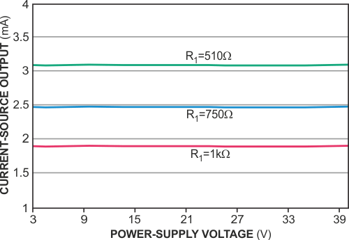
| Figure 2. | Setting R1 to values of 1 kW, 750 W, and 510 W delivers output currents of approximately 1.8, 2.5, and 3.6 mA that are insensitive to a wide range of power-supply voltages. |
|
Note that the circuit's lower power-supply-voltage limit must exceed the circuit's compliance voltage, 3 V, plus the voltage drop that the sensor introduces: ISOURCE × R2. The circuit's upper power-supply voltage must not exceed ISOURCE × R2 + 30 V. For example, supplying a current of 2.5 mA to a 1-kΩ pressure-sensor bridge, R2, limits the power-supply-voltage range to 5.5 to 32.5 V. The circuit's output current varies less than 1 µA over a wide range of power-supply voltages (Figure 2).