The power factor corrector (PFC) front end of an off-line power supply is subject to the operating frequency limitation caused by the Miller Effect of its associated power MOSFET. This effect is a property of any transistor configuration with a common source (MOSFET) or common emitter (bipolar transistor) configuration.
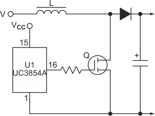
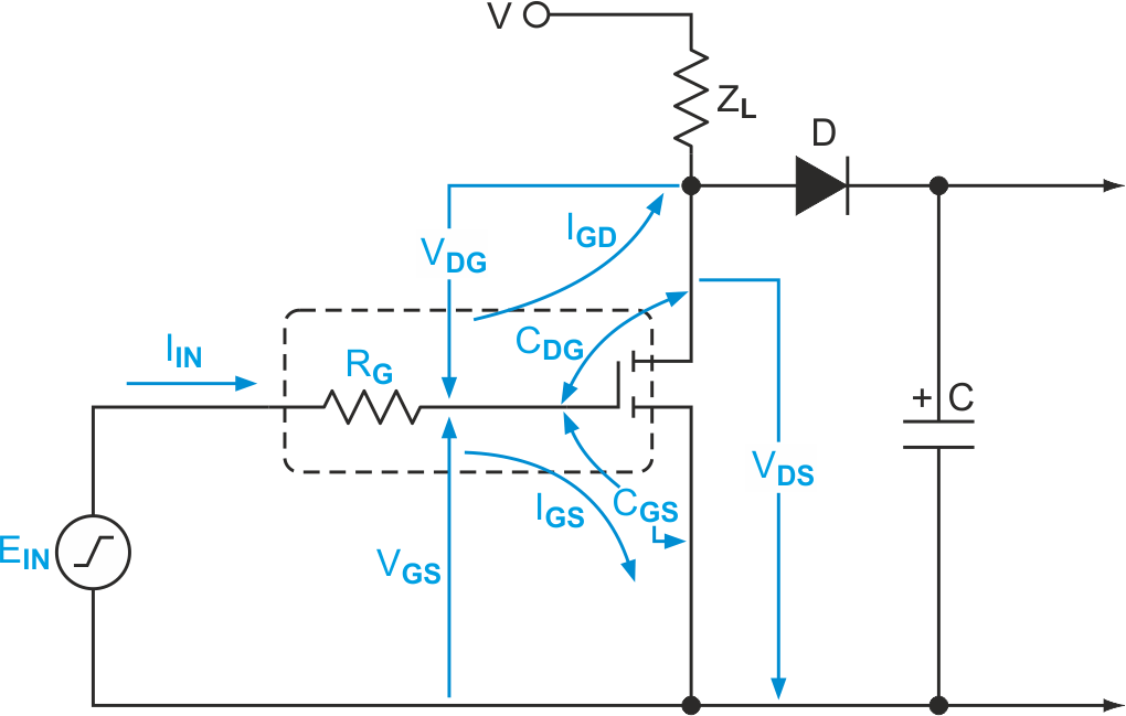
Most PFCs employ a boost converter based on a configuration with a common source MOSFET or common emitter power bipolar transistor. Figure 1 shows a conventional boost PFC kernel using a common source power MOSFET (Q). This is essentially a high gain amplifier that controls power by storing and releasing it into inductor L. During the MOSFET ON and OFF states, its drain voltage (VDS) swings between almost zero and PFC output, which is generally 200 to 400 V. This voltage periodically recharges the MOSFETs drain-to-source (CDS) and drain-to-gate (CDG) capacitances and affects the gate-to-source (CGS) capacitance (Fig. 2).
 |
||
| Figure 1. | This simplified PFC circuit uses the UC3854A and a single power MOSFET. |
|
It's important to keep in mind that the VDS and drain-to-gate voltage (VDG) are in counter-phase with respect to the VGS and EIN driving voltage. This means there is a negative feedback from the drain-to-gate, which is the Miller Effect. The Miller Effect increases the apparent input capacitance of a MOSFET or bipolar transistor.
 |
||
| Figure 2. | Here, input capacitances, voltages, and currents are given for a power MOSFET input circuit. |
|
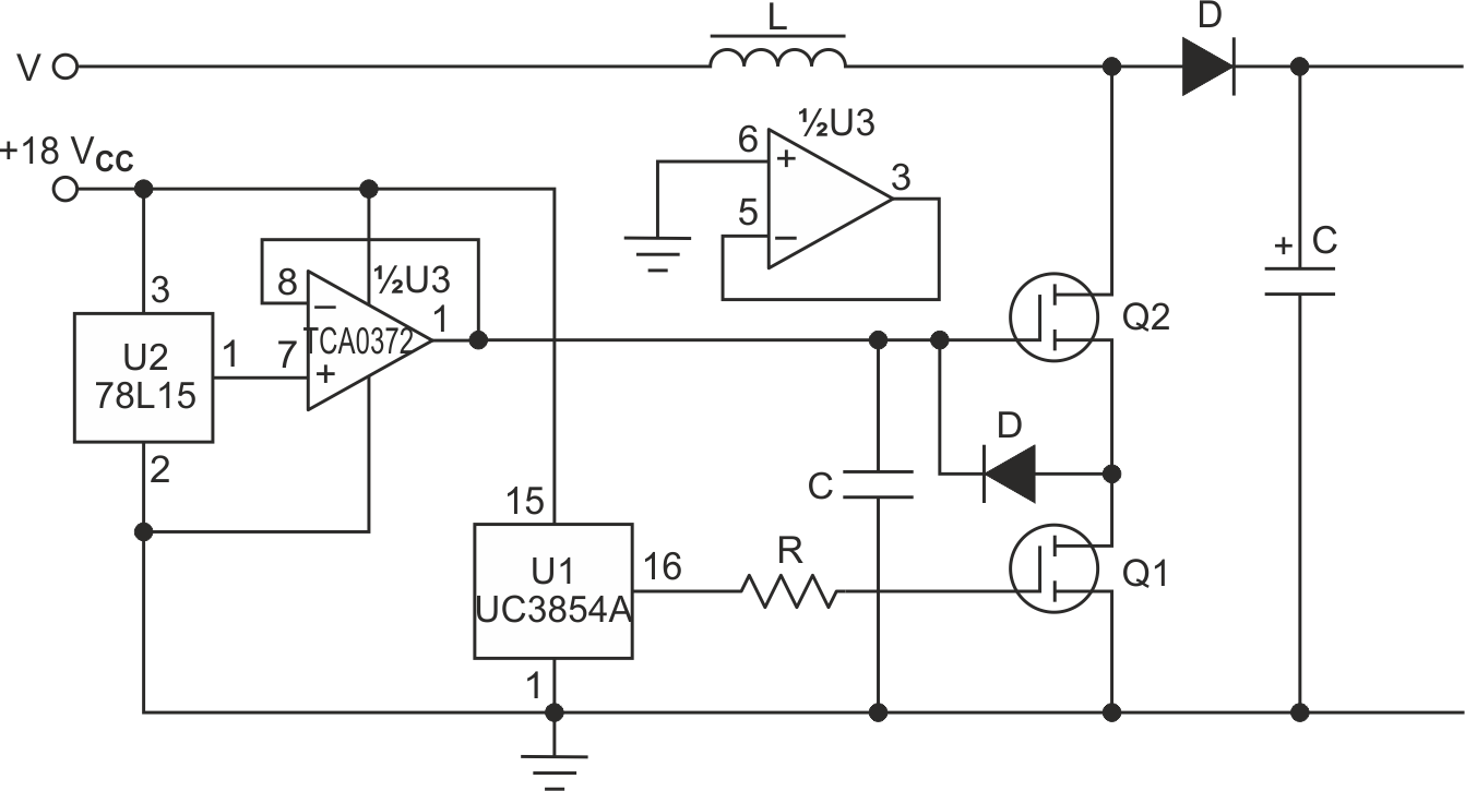
To solve for the Miller Effect, see Figure 3. It depicts a cascode amplifier employing boost controller U1 (Texas Instruments’ UC3854A may be a good implementation), driving a low-voltage and low-RDS MOSFET (Q1) through resistor R. This common source configuration has a very low-impedance drain load because high-voltage transistor Q2 is a common-gate configuration, and Q1 "sees" its source. In operation, the Q1 drain voltage swing is only about VCC, while the load is a very low impedance.
 |
||
| Figure 3. | In this common source configuration, the PFC circuit features cascode MOSFETs and uses boost controller U1 to drive a low-voltage MOSFET through a resistor. |
|
This doesn't trigger the Miller Effect due to a very low voltage gain of Q1. The upper high-voltage MOSFET Q2 has a common gate connection, which eliminates the negative feedback and thus the Miller Effect. This is why the apparent capacitance of Q2 is just the gate-to-source capacitance (and even less due to the positive feedback through Q2, CDS).
During operation, both Q1 and Q2 are either ON or OFF. When the Q2 drain voltage changes rapidly, it affects the gate and source networks through capacitances CDG and CDS. Diode D serves as a clamp for the Q2 source, connecting it to the VCC when Q2 turns off and its drain pulls up the source through the CDS.
It's worth mentioning that the Q2 drain seriously affects the Q2 gate circuit, which tends to change the VCC. To prevent this, the source of the VCC should be able to resist both pull-up and pull-down changes, providing substantial sinking and sourcing currents. The VCC source can be made upon a linear voltage regulator LM78L15 and an operational amplifier capable of producing output current of around 1 A.