In this article, we point out some important facts in designing RF application PCB boards. Of course there are many other facts that are not listed below but for the beginners these may be enough for now.
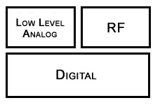
First of all, separate the analog , RF and digital parts of your system and try to design the PCB without mixing them. Likewise separate the RF stages like VCO, amplifier and etc. and don't draw one's line through one another's.
1) Surely use a multilayer PCB. If your PCB design includes only two layer, the top layer should include the power stage, RF signal lines and RF components. Then the bottom layer must be the ground plane.
2) The length of the lines that carry RF/Microwave signals is a very important issue. They should be at most 1/20 length of the wavelength. So there will be no loss. For instance, when we calculate for 433 MHz;
λ (Wavelength) = c (The Speed of Light) / f (Frequency)
λ = 300000000/433000000 = 69,28 cm
Max. Line Length : λ/20 = 3,46 cm
If the line must be necessarily longer, then impedance matching with L and C components must be applied at the end of the line.
3) If you use multilayer PCB, draw the short RF lines on the top layer. To reduce the noise, draw the power lines between two ground layers. There must be absolutely a ground layer under the layer that includes the RF signal lines.
4) Draw the RF signal lines quite separately. If they are adjacent to eachother, then crosstalk may occur. (Crosstalk : Undesired transfer of signals between or among two lines such as telephone lines, data lines, or system components. )
5) Use least number of vias in RF stage.
6) Connect the ground pins of the RF ICs to the ground plane as shortly as possible by using vias. You can use multiple vias to reduce the unwanted effects of the ground.
7) When you finish all the layers, fill the empty spaces with copper pour that is connected to the ground. Place vias that are connected to the ground layer with a distance of λ/20 cm between eachother.
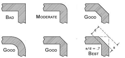
8) The proper corner drawings are shown below;
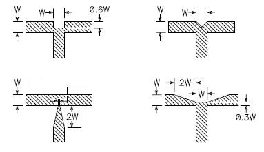
9) T shaped nodes should be like shown in the figure;
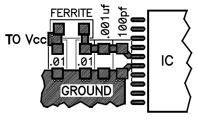
10) Decouple the supply voltage. An example circuit and its PCB is shown below. Consider that the capacitor with a smaller capacitance is placed nearer to the IC.
11) Coils generate strong magnetic fields around, place them quite seperate from eachother to prevent the interaction.