Mikhail Shustov, Tomsk
The operation principle is described and the diagrams of analog-digital frequency-dependent relays, whose switching occurs when the certain setting valuation input frequency is exceeded by frequency, are given.
Analog-digital frequency relays, considered in the article, are designed to respond to the executive or indicating device to exceed the specified limit value by the predetermined threshold controlled frequency. The undeniable advantage of such relays is that they can be easily configured to operate in the frequency range from units of Hz to hundreds of kHz.
 |
||
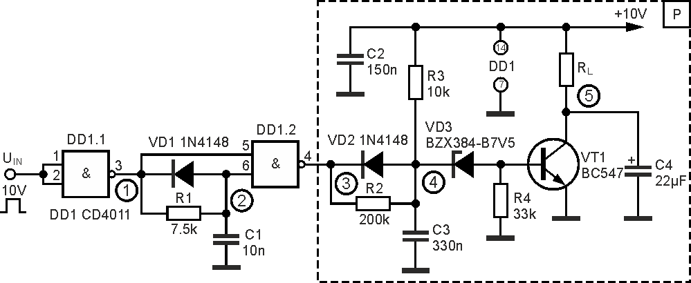
| Figure 1. | A single-channel analog-to digital frequency-dependent relay at f GR ≈ 10 kHz. | |
The operation of analog-to-digital frequency-dependent relays is based on charge-discharge processes in RC-circuits [1, 2]. Figure 1 shows one of the variants of the relay. CMOS-level input by duty cycle 2 is supplied to the logic element input DD1. 1 CD4011(K561LA7). An RC circuit determining the limit frequency of the relay operation is connected to this element's output. fCUT ≈ 10 kHz for the nominal values of the elements shown in the diagram. This frequency can be calculated by formula
The capacitor is charged exponentially at a logic unit presence at element output DD1. 1 and almost instantly discharged through diode VD1 at switching the logic element (see the diagram, figure 2).
 |
||
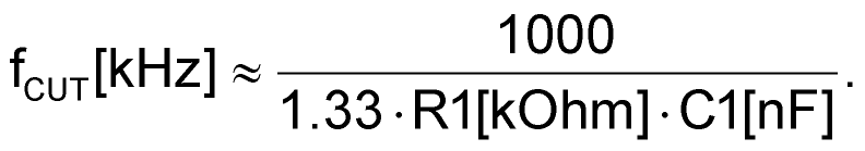
| Figure 2. | Diagrams of the signals at the device control points. | |
The second gating circuit DD1.2 serves as a comparator and, and at the same time, as NAND forming a logic output, whose duration increases with the input frequency. This signal, as well as the current through resistor R3, charges capacitor C3 of the second RC-circuit (R2C3) with a high logic output DD1.2, and instantly resets the capacitor charge through diode VD2, when the gating circuit is switched.
As a result, in the input frequency range f < f GR, the capacitor voltage C3 does not exceed the Zener breakdown voltage VD3 designed to reduce the probability of the output key cascade Maloperation. With the further frequency rise (see Figure 2), when the input pulse frequency reaches or exceeds f GR, at logic output DD1. 2 the logical unit will be constantly present, and the capacitor voltage C3 will reach the maximum value. The input key cascade on transistor VT1 will receive a control signal including the load (relay, led, etc.). The transition region of the switching rate for fCUT= 10 kHz is placed in a bandwidth under 100 Hz.
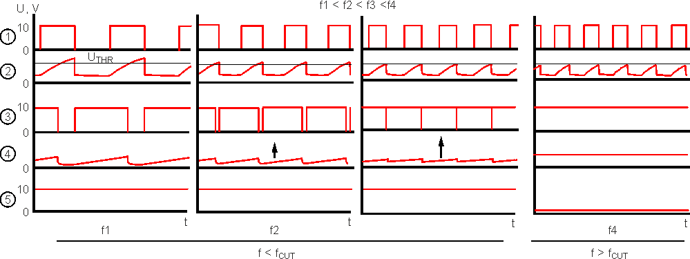
Figure 3 shows a diagram of a three-channel analog-to-digital frequency-dependent relay with previously unused CMOS-circuit logic elements CD4011 (K561LA7). Blocks Pf1-Pf3 are made identically (see. Figure 1) The cutoff frequency response of the first channel (10 kHz) remained unchanged, since the total resistance of resistor R1 and potentiometers R2, R3 being switched in parallel, remained unchanged (7.5 kOhm). The response frequencies of the rest channels can be continuously adjusted upwards by potentiometers R2 and R3.
Among no major deficiencies in the relay, their response can be included if the input frequency goes down 0.01fCUT. This frequency is determined by the chain time constant R2C3, Figure 1.
 |
||
| Figure 3. | Three-channel analog-to digital frequency relay. | |
The number of relay channels can be significantly expanded by the solution shown in Figure 3. As mentioned above, the frequency rates of the relay operation can be adjusted in one or the other direction by the proportional action of the RC-circuit values.