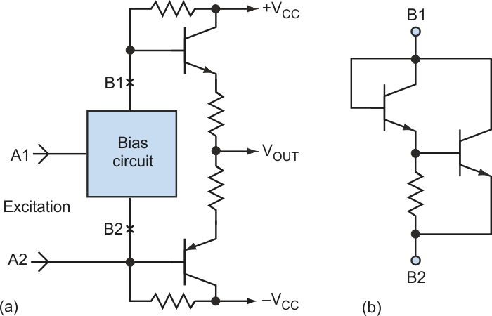
Bias circuits for class AB buffers (Fig. 1a) can take several forms. One alternative (not necessarily the best) is usually called the “old VBE doubler” (Fig. 1b).
 |
||
| Figure 1. | The typical class AB buffer (a) can use a number of bias circuits, including the VBE doubler (b). |
|
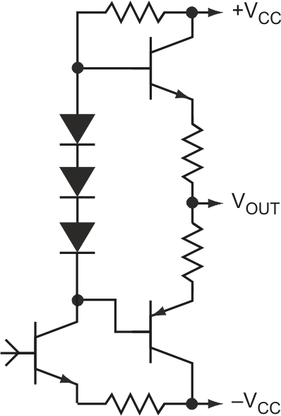
The main purpose of these circuits is to provide VCC-independent (and very often thermally compensated) bias for output transistors, so every effort is made in this direction. But you should also consider signal quality. The nonlinearities of the devices involved (as, for example, in the bias circuit in Figure 2) will make a noticeable contribution to the total harmonic distortion (THD) of the buffer.
 |
||
| Figure 2. | The nonlinearities of devices used in some bias circuits, such as this one, can cause distortion in the amplified signal. |
|
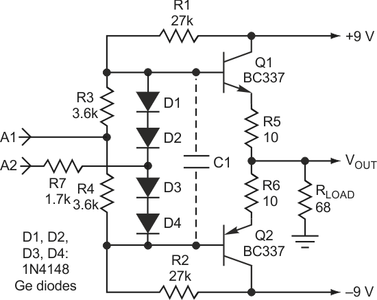
Indeed, direct measurements show for symmetrical excitation through A1 (Fig. 3) that THD = 0.13%. The far more common asymmetrical (unbalanced) excitation through A2 raises THD to an awful 0.43%, due to a significantly higher second harmonic in the output spectrum.
 |
||
| Figure 3. | This circuit illustrates two bias possibilities. Symmetrical excitation through A1 creates a THD = 0.13%. The more common asymmetrical excitation through A2 produces a THD = 0.43%. |
|
To avoid these distortions, capacitor C1 often is added. But to work properly, C1’s impedance at the lowest frequencies must be many times lower than the dynamic resistance of the bias circuit, which itself may be quite low. As a result, this technique usually isn’t practical, especially for integrated amplifiers.
To eliminate the influence of the bias circuit on the amplified signal spectrum, you can add two matching resistors – R3 and R4 – to balance the bridge circuit R1/R2/R3/R4 (Fig. 3, again). Of course, this bridge should use low-value resistors to minimize the influence of the input impedances of Q1 and Q2. Also, high-beta transistors are highly preferable in this case.
Properly balanced, both terminals of the bias circuit will have the same ac level, eliminating ac flow through it. The result is a sharp drop in distortion, with a THD of only 0.05%. What’s more, R3 and R4 tend to maintain the stability of the Q1, Q2 follower, especially with the capacitive load.
 |
||
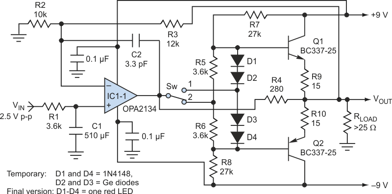
| Figure 4. | The typical class AB buffer (a) can use a number of bias circuits, including the VBE doubler (b). In this test circuit, with the switch at position 1 (usual bias circuit) and a heavier load (25 W at 6 V), THD = 0.022%. With the switch at position 2 (the improved bias circuit), THD = 0.007%. |
|
Figure 4 shows one half of a headphone stereo amplifier with THD < 0.005% at VOUT = 3 V p-p and a 60-W load. To compare the usual and the novel circuits, switch Sw is added; it is omitted in a practical circuit and diodes D1-D4 can be substituted with one red LED. With a more typical heavier load (25 W at VOUT = 6 V) and the switch at position 1 (usual circuit), THD = 0.022%. In contrast, the novel circuit (switch at position 2) produces a THD of only 0.007%.