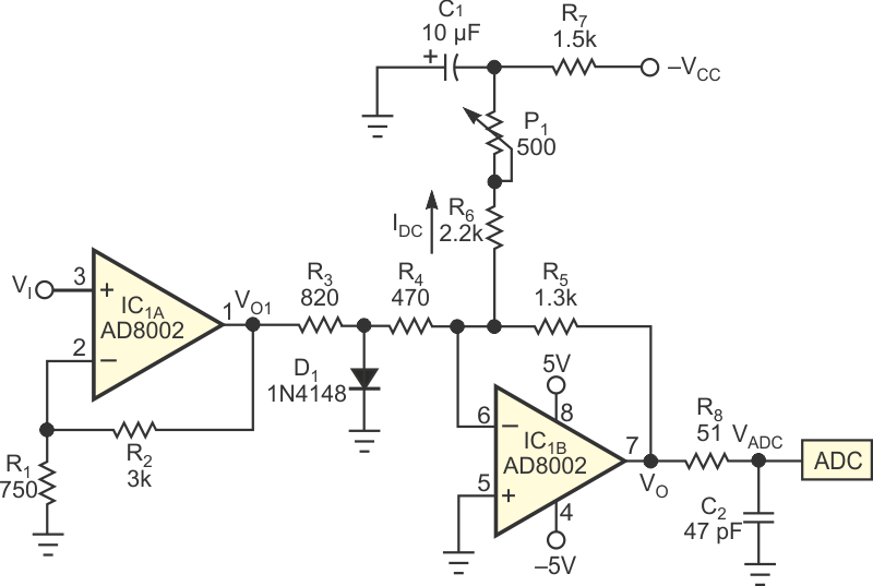
Many flash ADCs, such as Texas Instruments' ADC1175, have a recommended operating input-voltage range of 0.6 to 2.6 V. However, in some applications, you must convert a symmetrical analog-input signal. The circuit in this Design Idea converts a symmetrical input-voltage range of –0.2 to +0.2 V into the recommended 0.6 to 2.6 V range (Figure 1). The circuit also prevents the output voltage from going below –0.3 V, which would probably damage the ADC.
 |
||
| Figure 1. | Adding R3 and D1 to a conventional op-amp circuit provides clipping. R3, D1, R4, and R5 determine the clipping level. In addition, adding the IDC current causes dc-shifting of the output voltage. |
|
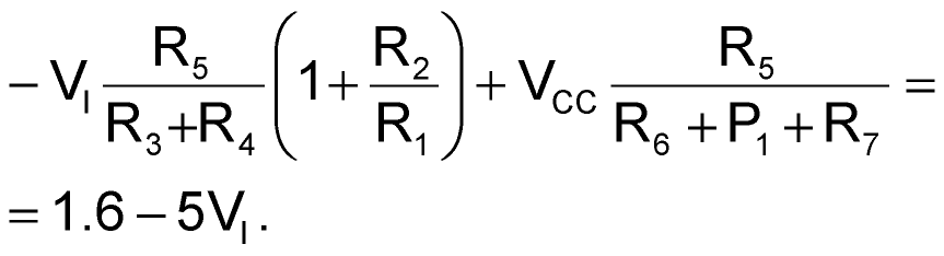
The circuit uses an Analog Devices AD8002 dual-current-feedback operational amplifier to obtain a high bandwidth. The first block, noninverting amplifier IC1A has a voltage gain of five. This block also provides high input impedance and low output impedance, so that the second block, IC1B, operates properly. The second block does most of the work. Starting from a basic inverting amplifier comprising IC1B, R4, and R5, you obtain the clipping effect by adding R3 and D1. R3, D1, R4, and R5 determine the clipping level. In addition, adding the IDC current dc-shifts the output voltage. You can trim adjustable potentiometer resistor P1 to obtain the desired output voltage shift – that is, 1.6 V.
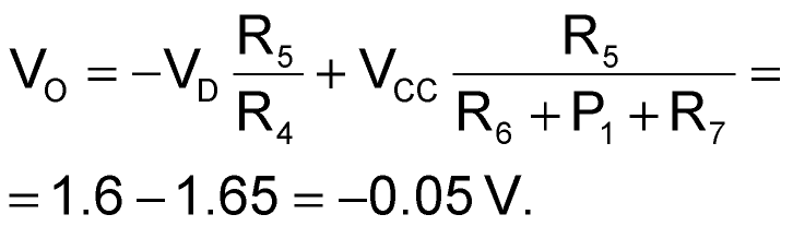
If diode D1's current is negligible, the output voltage, VO, is
Given that the diode voltage, VD, is 0.6 V,
The clipping takes place near 0 V, protecting the ADC. Raising the clipping level makes the circuit less linear in the nonclipping range. In other words, a design trade-off exists between clipping level and linearity. Resistor R8 limits the current through the ADC's input pin. Capacitor C2 is optional; it limits the VADC/VI bandwidth. Capacitor C1 helps to reduce the voltage noise that might come from the –VCC power supply.