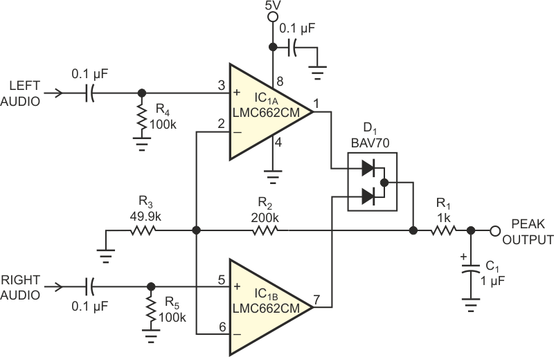
The simple peak detector in Figure 1 is the result of a need for a single-5V-supply, level/clipping indicator for a multimedia-PC sound system. The design is unique in that it detects both stereo channels on a single peak-hold capacitor. All the adjustments in the circuit simultaneously apply to both left and right stereo inputs. The output is suitable for driving a bar-graph display or for analog-to-digital conversion and display with a microprocessor. The circuit operates as a dual positive-peak-detector circuit. The dual diode, D1, serves to allow positive peaks to pass while disconnecting the op amp from the hold capacitor, C1, on negative peaks. Also, because the diodes have an OR connection, the circuit detects only the larger peak from the left or right stereo input. The values shown in Figure 1 are for standard 200-mV-rms line-input levels, such as those you'd find on a PC's sound-card line input. Your personal preference or exact needs might require other performance parameters, and you can easily adjust these values.
 |
||
| Figure 1. | This simple circuit provides peak detection and clipping indication for a PC’s stereo channels. | |
The gain for both stereo channels is equal to 1+R2/R3. The circuit as shown has a gain of 5. For a full-scale 200-mV- rms input, this gain produces an output of approximately 1.4 V. This value is convenient for this application, which uses three green LEDs, two yellow LEDs, and one red LED to show the relative peak levels of the stereo channels. Nominal, full-scale line input of 200 mV rms lights two of the green LEDs. “Attack time” is the time it takes the peak detector to respond to 69% of an input-signal peak, or one time constant. The time constant R1C1 sets the attack time. In this circuit, the attack time is 1 msec. The decay time is the time it takes the peak to decay to 31% of its original value, or one time constant. This time equals (R2 + R3)C1 (assuming that R1 is negligibly small compared with R2 + R3). The decay time in this case is 250 msec, because that value produces a pleasing-looking bar-graph display. Some applications may need different response rates; you can easily obtain them by following the design equations above.