The increasing acceptance of Class D amplifiers has helped them gain market share from their linear Class AB brethren. That acceptance is no surprise; the advantages of Class D amplifiers are legion, but such amplifiers also require new techniques for evaluation. For example, consider a basic sine-wave test of a linear amplifier. You apply power, apply a sine wave of suitable amplitude to the input, and connect an oscilloscope probe to the output. You'll see a replica of the input, usually offset by about half the power-supply voltage. Even if the linear amplifier drives a BTL (bridge-tied load), you'll still see a recognizable replica of the input at either end of the load, albeit at half of the output signal that's available.
Testing a Class D amplifier poses more difficulties. The amplifier's output comprises a PWM (pulse-width-modulated) signal that swings between ground and the supply voltage at a frequency that's usually 200 kHz to 2 MHz. However, when you view this PWM output on an oscilloscope, you'll see no resemblance to the sine-wave input.
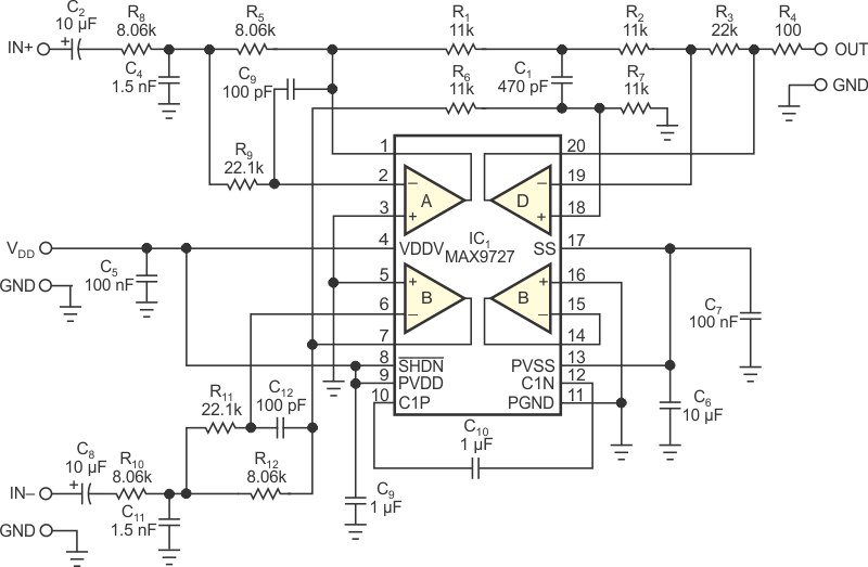
You can observe a Class D audio amplifier's output if you introduce the filter circuit in Figure 1. Based on Maxim's MAX9727 quad-audio-line driver, IC1, the circuit combines separate single-ended filters – one for each of the BTL outputs' phases – with a third amplifier that provides a difference signal with additional filtering. The first stage of each single-ended-filter section contributes the complex-conjugate pole pair of a third-order, 30-kHz multiple-feedback Butterworth filter, for which many design guidelines and equations are available. Each third-order-filter section comprises a complex-conjugate pole-zero pair and one real pole.
 |
||
| Figure 1. | Use this third-order, 30-kHz filter circuit to observe a Class D amplifier’s output signal on an oscilloscope. | |
To improve the match between the signal paths, the two separate multiple-feedback filters share a real pole, which 470-pF capacitor C1 and 11-kΩ resistors R1 and R6 provide. The circuit implements that pole as a difference amplifier, thereby producing a filtered output that presents a single-ended version of the BTL amplifier's outputs. The filters' signal paths present 5.5-kΩ impedances to each of the A and B amplifier sections' inputs. By inspection, the net 5.5-kΩ impedance from Section B's output to C1 comprises the Thevenin-equivalent impedance of resistors R6 and R7. Similarly, the net impedance from Section A's output to C1, also 5.5 kΩ, comprises the Thevenin impedance of resistors R1 and R2. Note that the virtual ground from Amplifier D's inverting input effectively grounds resistor R2.
Matched resistors attenuate each of Amplifier D's differential inputs by 6 dB (IN+ by R1 and R2 and IN– by R6 and R7). A 22-kΩ feedback resistor, R3, provides Amplifier D with a gain of two, which sets a unity-gain-transfer function in the circuit's passband. The circuit's single-ended output with respect to ground allows the oscilloscope's ground to also serve as the output signal's ground. A version of this circuit using conventional op amps would require a negative-power-supply-voltage source, but Maxim's MAX9727 already includes a negative-voltage source, which its internal charge-pump circuit generates. When you operate the circuit from a 5 V supply, the circuit's output delivers more than 2.5 V rms. Although its third-order filter is inadequate for precise measurements of distortion or noise, the circuit provides an excellent tool for troubleshooting and evaluating Class D-amplifier circuits and inspecting their outputs on an oscilloscope.