Ferran Bayes
EDN
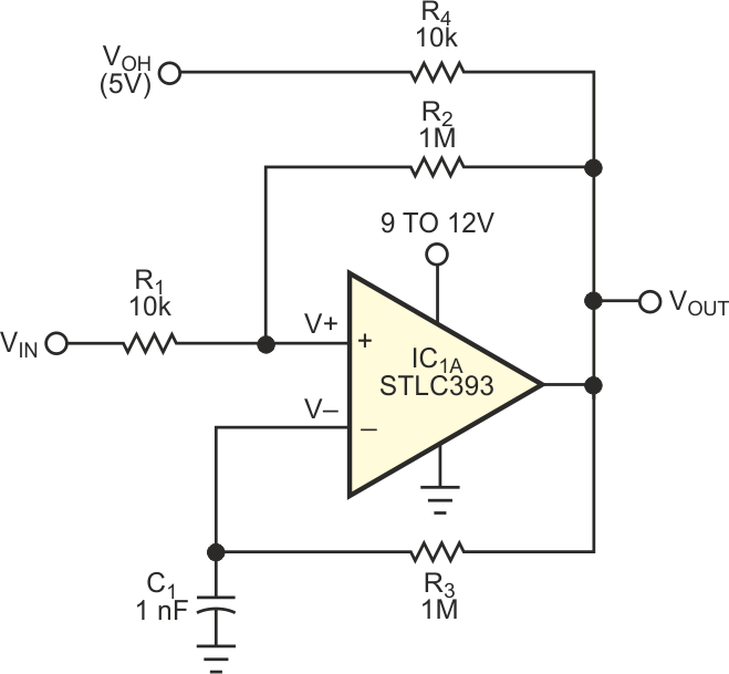
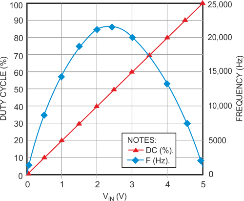
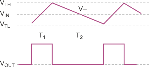
A previous design idea is reminiscent of a similar but somewhat simpler circuit (see [1]). This circuit delivers a rectangular signal with duty cycle varying between 0 and 100% in response to an input signal varying from 0 to 5 V dc (Figure 1). As with the above-mentioned circuit, the frequency is not constant (Figure 2), but the circuit is so simple that it can be useful in certain applications. In response to the hysteresis R2 provides and the time constant R3C1, the comparator delivers the rectangular wave (Figure 3). The voltage V– at the inverting input swings between the two threshold levels, VTH and VTL. If you assume that R2 >> R1, then V+ is always very close to VIN. R3C1 averages the signal at VOUT, and the dc voltage at V– is proportional to the duty cycle of VOUT. The closed feedback loop tries to make V– equal to V+; therefore, the duty cycle at VOUT is proportional to VIN.
 |
||
| Figure 1. | This voltage-controlled PWM circuit is simplicity personified. | |
 |
||
| Figure 2. | Output frequency is a nonlinear function of the input voltage. | |
 |
||
| Figure 3. | The voltage at the inverting input follows a linear ramp. | |
The voltage at VOH determines both the output signal's high level and the full-scale range of VIN. It can have any value, insofar as it does not surpass the common-mode input range of the comparator. The mathematical analysis of the circuit is easy if we assume that, because VTH – VTLis small, we can approximate the exponential charge and discharge of C1 to assume the characteristic stemming from a constant-current source/sink. During the charging phase, the current is approximately (VOH – VIN)/3, so:
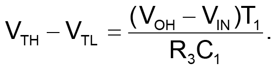
Similarly, during the discharge phase, we can assume the current is VIN/3, and
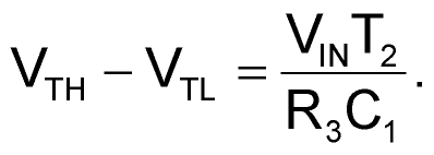
Matching the two equations yields
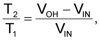
and the duty cycle, D, is
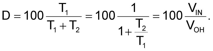
You can see that the duty cycle is directly proportional to VIN: 0% for VIN = 0 V and 100% for VIN = VOH. Moreover, the duty cycle is essentially independent of the component values, with the constraint that R2 >> R1 to keep hysteresis small. An inverse relationship between duty cycle and VOH can be useful in some applications, so consider VOH as an additional input. The output frequency follows the relationship
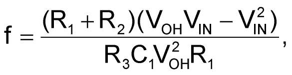
reaching its maximum at VIN = VOH/2.
Tests with a TLC393 CMOS comparator and a bipolar LM393 reveal that the TLC393 performs better at low values of VIN, because of its lower VOL. Avoid loading the comparator's output; buffer it if necessary, because the loading can degrade the switching levels.