A previous Design Idea [1] outlined a relatively simple circuit in which a momentary pushbutton could be made to function like a latching, mechanical switch. The article generated a good deal of reader feedback. Amongst other comments, readers questioned whether it would be possible to adapt the circuit to provide (a) a cross-coupled arrangement in which two switches could be made to ’cancel’ each other; and (b) a ’time delay’ version in which the circuit would turn off after a predetermined time had elapsed. This idea attempts to address each of these suggestions.
Cross-coupled, latching switches
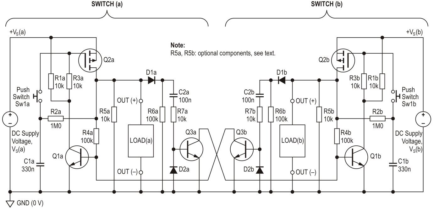
Figure 1 shows two switch circuits connected in a cross-coupled fashion where each switch is turned on and off by its own momentary pushbutton, and is also switched off whenever the other switch is turned on. This mutual cancelling behavior lends itself to applications such as automotive indicators.
 |
|
| Figure 1. | Cross-coupled switches latch on independently but cancel each other. |
The two switch circuits are identical and mirror each other, i.e., R1a provides the same function as R1b, Q1a behaves exactly like Q1b, and so on. Furthermore, except for the additional cross-coupling components (C2, D1, D2, R6, R7, and Q3), each circuit is largely identical to the one shown in Figure 1(a) of the previous Design Idea where you’ll find a detailed description of how the basic circuit functions. Remember that R5 may or may not be necessary depending on the nature of the load, and that for loads such as motors it may be necessary to fit a blocking diode between the OUT (+) terminal and the load.
To understand how the cross-coupling works, assume that switch (a) is currently off, and switch (b) is on, such that Q1a and Q2a are off, and Q1b and Q2b are both conducting and providing bias for each other via R3b and R4b. If momentary pushbutton Sw1a is now pressed, Q1a and Q2a switch on, and switch (a) latches into its energized state. At the moment Q2a switches on, a pulse of current is delivered to the base of Q3a via D1a, C2a, and R7a causing Q3a to switch on momentarily, which briefly shorts Q1b’s base to 0 V. Both Q1b and Q2b now turn off and switch (b) latches into its off state. Switch (a) is now latched in its energized state and the switches will remain in this state until either of the push switches is pressed. So, if Sw1b is now pressed, Q1b and Q2b switch on, switch (b) latches into its energized state and Q3b momentarily switches on causing Q1a and Q2a to switch off.
The length of time for which Q3 is briefly pulsed on is determined by the C2-R7 time constant and must be long enough for the opposite MOSFET to turn off completely. Remember that when Q1 turns off, the charge stored on Q2’s gate must be removed completely via R1 in series with R3. Some ’large’ (high current) MOSFETs have gate capacitances of tens of nanofarads, so with R1 = R3 = 10 kΩ it can take several milliseconds for the gate to discharge completely. Now, with C2 = 100 nF and R7 = 10 kΩ, Q3 clamps Q1’s base for around 5 ms which should be long enough to turn off the majority of P-channel MOSFETs.
At the end of the current pulse described above, the voltage stored on C2 will be roughly equal to the supply voltage, +VS. Without diode D1, this voltage would hold Q1 on, thereby preventing the switch from turning off. With D1 in circuit, the blocking action allows the switch to turn off normally, such that when Q2 turns off, the voltage on C2 discharges via the path formed by R6-D2-R7.
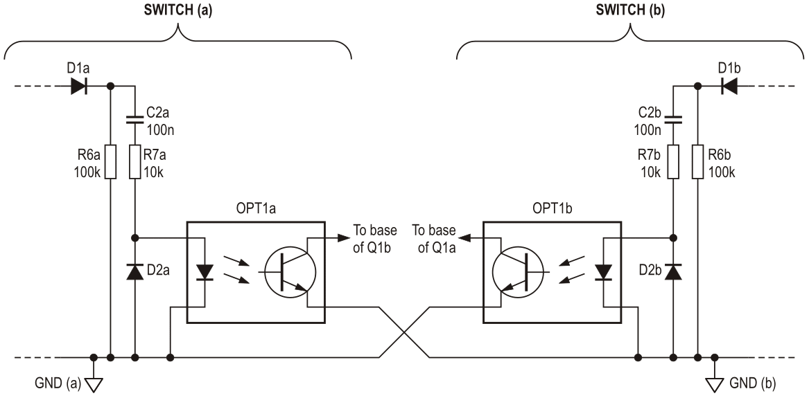
Although switch (a) and switch (b) are identical, they do not need to share the same supply voltage, i.e., +VS(a) and +VS(b) do not need to be equal and can be derived from different sources. However, for the circuit in Figure 1 to achieve cross-coupling, switch (a) and switch (b) must share a common ground return (0 V). For applications where this is a problem, Q3a and Q3b can be replaced by optocouplers (Figure 2), which allows each switch to have its own ground return, galvanically isolated from the other. Most common-or-garden optocouplers should work perfectly well, but remember that the opto’s LED requires more drive voltage than a transistor, so it may be necessary to reduce the value of R7 (and increase C2 accordingly) if the supply voltage, +VS, is fairly low.
 |
|
| Figure 2. | Optocouplers allow for completely isolated cross-coupled switches. |
Latching switch with timed output
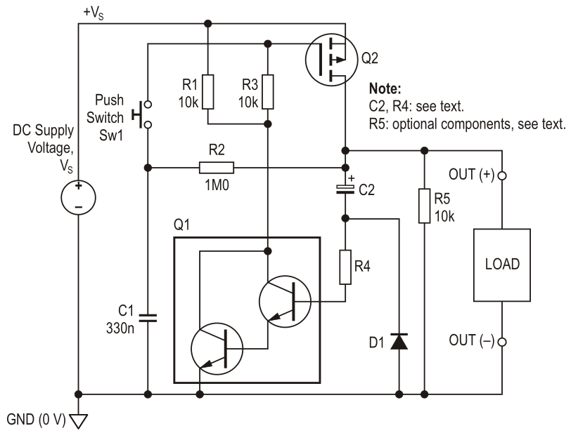
Certain applications may require a latching switch that turns off automatically after a preset period of time. A fairly simple way of achieving a timed output is shown in Figure 3, where Q1 has been changed from a single transistor to a Darlington pair, and capacitor C2 has been inserted between Q2’s drain and R4. As before, a momentary pushbutton, Sw1, is used to control the circuit. When the switch is closed, Q2 turns on and sources bias current to the Darlington’s base via C2 and R4. The circuit now latches into its energized state with Q2 held on via Q1.
 |
|
| Figure 3. | Minor changes to the basic switch circuit allow for a preset timed output. |
C2 now begins to charge and the voltage at the junction of C2 and R4 falls at a rate largely determined by the C2-R4 time constant. As this voltage falls, so does the base current delivered to the Darlington via R4; eventually, the Darlington’s collector current becomes too small to provide sufficient gate drive for Q2 and the MOSFET switches off. The switch now reverts to its unlatched state and C2 discharges via D1 and the load in parallel with R5 (if fitted). Note that the switch can be unlatched at any point during the timed ’on’ period simply by pressing the pushbutton – it is not necessary to wait until the output has timed out.
The high current gain afforded by the Darlington pair allows for large values of R4 (on the order of several megaohms) to be used to produce a long time constant. A test circuit powered from a 15 V supply generated an ’on’ time ranging from around nine seconds with C2 = 1 µF and R4 = 1 MΩ to just over 15 minutes with C2 = 10 µF and R4 = 10 MΩ. Increasing C2 to 100 µF resulted in an ’on’ time well in excess of two hours.
References
- Anthony Smith, “Latching power switch uses momentary pushbutton.”