Converting band-limited NRZ (non-return-to-zero) data to a digital format suitable for microprocessors and other digital systems poses problems when a signal's duty cycle or amplitude varies or when its average level unpredictably wanders within a given dc range. Transferring the signal to a fixed-reference comparator using ac coupling produces poor results because changes in duty cycle cause variations in average signal level that result in jitter or distortion of the output signal's timing.
Based on diodes and RC networks, an envelope tracker creates a voltage between the input signal's excursions (Reference 1). Using the midpoint voltage as a reference, the comparator generates a digital output signal that faithfully replicates the original signal's timing information. Although highly effective for relatively large signals, a diode-based circuit can introduce errors or even fail completely for inputs that are small relative to a diode forward-voltage drop or when the input's average level drifts toward either of the circuit's supply-voltage rails.
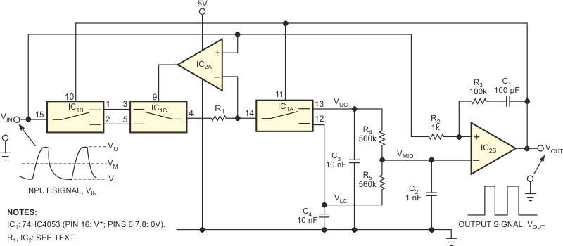
Requiring no diodes, the single-supply circuit in Figure 1 reconstructs a band-limited NRZ data stream whose duty cycle can vary from less than 5% to more than 95% and whose amplitude varies from less than 100 mV to the supply-rail voltage – 5 V, for example. Furthermore, the circuit tolerates an average signal level that falls between the two supply rails. The circuit comprises triple analog switch IC1, dual comparator IC2, and a few passive components.
 |
||
| Figure 1. | This circuit tracks an NRZ signal’s envelope excursions and recovers the original waveform. | |
The circuit functions as a self-clocking envelope tracker by sampling the input signal's upper and lower levels, VU and VL, and generating corresponding dc levels, VUC and VLC, on capacitors C3 and C4. Two equal-valued resistors, R4 and R5, between C3 and C4, produce a third voltage, VMID, that's equivalent to the input signal's midlevel voltage, VM. Capacitor C2 smoothes and filters VMID, which serves as a reference potential for output comparator IC2B. R2, R3, and C1 provide temporal hysteresis, ensuring clean switching of VOUT, even for relatively small inputs.
To understand the circuit's operation, assume that C4, C2, and C3 all discharge; that is, VLC, VMID, and VUC are all 0 V. Because input signal VIN is greater than VMID and the potential at IC2A's inverting input, both comparators' outputs go high and cause the three analog switches to assume the positions in Figure 1. Now, assume that VIN is at its positive peak amplitude, VU. Capacitor C3 now charges through R1 and the on-resistances of the three switches. Provided that C3 is not too large, VUC rapidly acquires a value roughly equal to VU.
When VIN falls below VUC, comparator IC2A's output goes low and forces analog switch IC1C to change state and disconnect C3 from VIN. Ignoring comparator input-bias currents and assuming negligible switch-leakage currents, C3 can now discharge only through R4. If R4 is large enough, the relatively slow discharge rate allows VUC to remain roughly equal to VU.
During C3's charging interval, C2 also charges through R4. Depending on the values of C2 and R4 and on the duration of the input signal's positive-going pulse, voltage VMID may exceed the input signal's lower level, VL. If VMID exceeds VL, comparator IC2B trips when VIN approaches VL, and the resulting low level at VOUT causes both IC1A and IC1B to change state. Capacitor C4 now connects to VIN through R1 and the switches' on-resistances and quickly charges to a level at which VLC approximately equals VL.
Depending on component values and on the input signal's timing parameters, several cycles may elapse before the circuit's voltage levels stabilize at their quiescent values, at which VUC≈VU, VLC≈VL, and VMID≈VM. However, careful selection of components ensures that the circuit rapidly reaches equilibrium. Ensuring that the comparator trips properly when VIN goes below VU or above VL requires that R1 provide a minimum amount of impedance of 100 Ω to 1 kΩ between VIN and IC2A's inverting input. Higher values result in sluggish charging of C4 and C3. In many designs, the combined on-resistances of IC1B and IC1C may allow omission of R1.
The presence of IC1B, IC1C, and IC2A ensures that C3 can charge when VIN is close or equal to VU and that C4 can charge only when VIN is close or equal to VL. Without IC1B, IC1C, and IC2A – that is, with VIN connected directly to R1 – C3 would discharge on the downward slope of VIN between VU and VM and would thus pull down VUC. Similarly, C4 would continue to charge on the upward slope of VIN between VL and VM and would thus pull up VLC. Although VMID might be roughly equal to VM, such a minimal configuration performs relatively poorly, particularly for small signals and at extreme duty cycles.
The components in Figure 1 produce good results for input frequencies of 5 to 50 kHz. Frequencies lower than 5 kHz may require larger capacitor values, and operation higher than 50 kHz may require reduction of capacitors' values and selection of a comparator with minimal response time. With properly selected components, the circuit performs well at baud rates to or exceeding 128 kbps.
The values of R5, R4, C2, and, to a lesser extent, the analog switches' on-resistance and R1, C4, and C3 determine the circuit's response time to a sudden change in input-signal amplitude or average level. Making C2 approximately 10 times smaller than C4 and C3 ensures a rapid "attack" time, but too small a value can result in excessive ripple and noise on VMID. For reliable operation, use equal values of close-tolerance resistors of 100 kΩ to 1 MΩ for R4 and R5. If you use high-value resistors for R4 and R5, choose a comparator with low input-bias currents for IC2. For detection of signals that might approach the positive-supply rail, the 0 V rail, or both, make sure that IC2 offers rail-to-rail input capability. Bypass each IC's power-supply connections with low-impedance ceramic capacitors.
 |
||
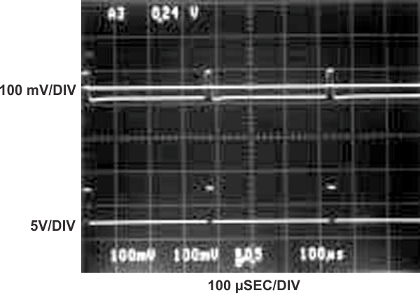
| Figure 2. | The lower trace shows the envelope tracker’s response to a bandwidth- limited, low-duty-cycle, low-amplitude input signal. The horizontal line in the upper trace shows the signals’ recovered midpoint voltage, VMID. |
|
Note that, with no input signal present (that is, when applying a dc level to VIN) VOUT may contain random pulses caused by noise and the comparators' attempts at maintaining VMID equal to VIN's average dc level. To eliminate the pulses, remove C1 to replace temporal hysteresis with "normal" hysteresis, but ensure that the hysteresis levels that R2 and R3 set are not excessively large relative to the minimum input-signal amplitude.
 |
||
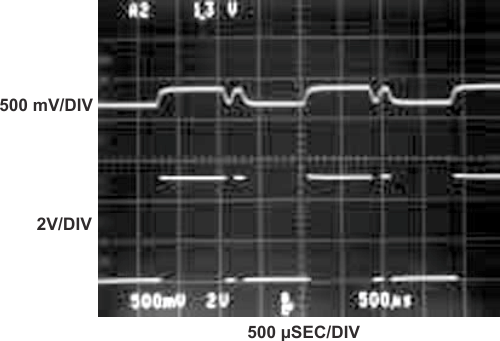
| Figure 3. | The lower trace shows the envelope tracker’s output signal recovered from an inductively coupled data transceiver. |
|
Figure 2 shows the circuit's response to a bandwidth-limited input signal of approximately 5% duty cycle and 75-mV amplitude. The horizontal trace, VMID, neatly bisects the waveform. The bottom trace shows the reconstructed signal at VOUT. In Figure 3, the circuit processes the real-world output of an inductively coupled transceiver (upper trace) of approximately 200 mV p-p. Again, the lower trace shows the reconstructed signal at VOUT.
Reference
- Whipple, Roger C, "Envelope tracker quells jitter", EDN, July 7, 1994, pg 102.