Gheorghe Plasoianu
EDN
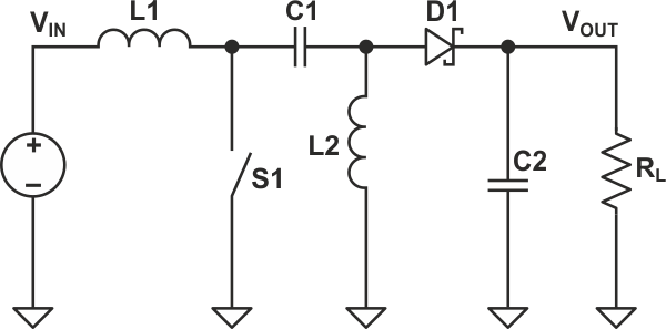
The single-ended primary-inductor converter (SEPIC) is a well-known type of DC/DC converter that, in its standard form, can generate an output voltage greater than, less than, or equal to its input voltage, and of the same polarity. This makes it particularly useful in battery-powered applications where the battery voltage starts higher but ends lower than the desired regulated output.
 |
||
| Figure 1. | Standard form of a SEPIC converter. | |
In its standard form, the SEPIC design's control device (usually a MOSFET, represented in the Figure 1 by the switch S1) sets the output voltage according to its duty cycle (D). Output follows the conversion ratio:
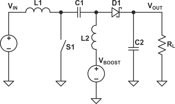
It is also possible, when desired, to offset the output voltage by connecting the lower end of L2 to a DC voltage (VBOOST), as shown in the Figure 2.
 |
||
| Figure 2. | SEPIC converter with an output voltage booster. | |
The output voltage in this configuration will be:
Variation 1
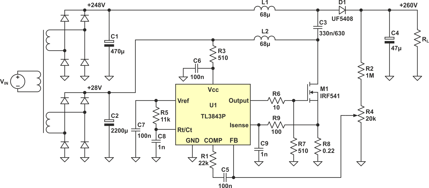
Because the control element is only working with a portion of the output voltage, it is possible to use this approach to regulate a voltage much higher than MOSFET's voltage handling capability. The schematic in the Figure 3 shows a working design, with the boosting voltage provided by the upper secondary of the transformer. The benefit of this regulator, in contrast to other similar approaches, is that the boost and the variable voltages have the same ground. It should be noted, though, that while the MOSFET does not need high voltage capability, though, the series capacitor C3 does.
 |
||
| Figure 3. | Full design of a SEPIC converter with high voltage output boost. | |
The circuit provides good regulation even with a changing load. In tests, changing the load current between 20 mA and 200 mA only caused the output voltage to drop by 0.5 V.
Variation 2
 |
||
| Figure 4. | Dual output bipolar SEPIC converter. | |
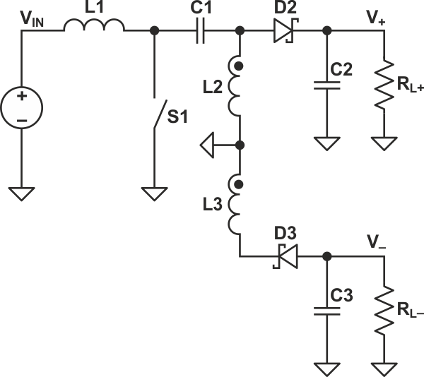
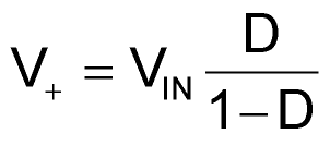
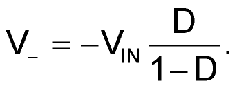
The variant of the conventional SEPIC converter shown in the Figure 4 provides two equal voltages of opposite polarity, with:
and
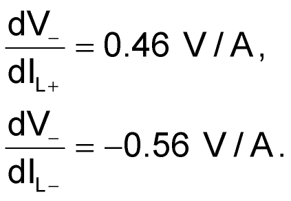
Compared to a previously presented Ćuk-SEPIC combined converter [1] it has a much better cross-regulation between the two output voltages. The two inductors L2 and L3 should be carefully coupled, however, to avoid voltage ringing at the cathode of D2. Otherwise, a suitable snubber must be used. A practical implementation of the approach is shown in the Figure 5.
 |
||
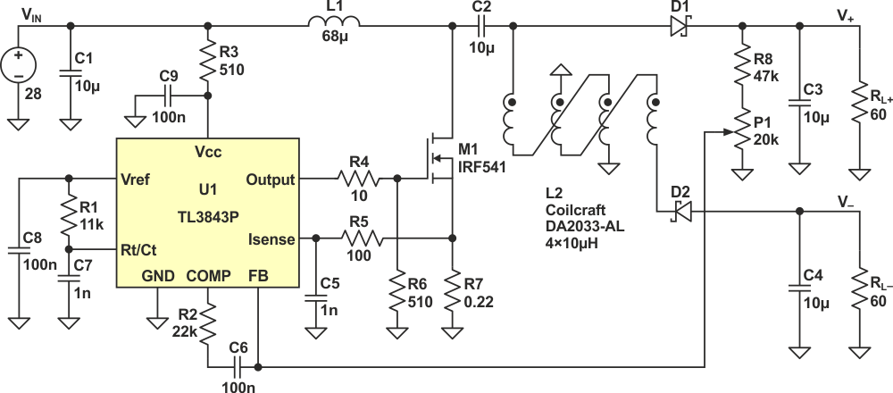
| Figure 5. | Practical implementation of a dual output SEPIC converter. | |
Testing the converter with differing loads yielded the results, shown in Table 1. With:
| Table 1. | Converter test results | ||||||||||||||||||||||||
|
|||||||||||||||||||||||||
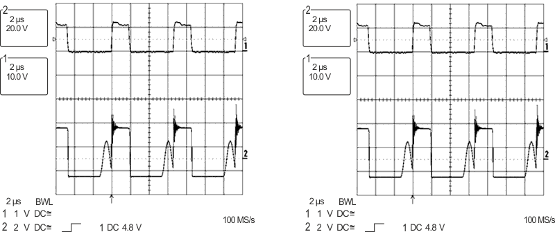
In the Figure 6 are the waveforms at the MOSFET gate and, respectively, cathode of D2 and anode of D1.
 |
||
| Figure 6. | Waveforms at MOSFET gate versus cathode of D2 (a) and anode of D1 (b). | |