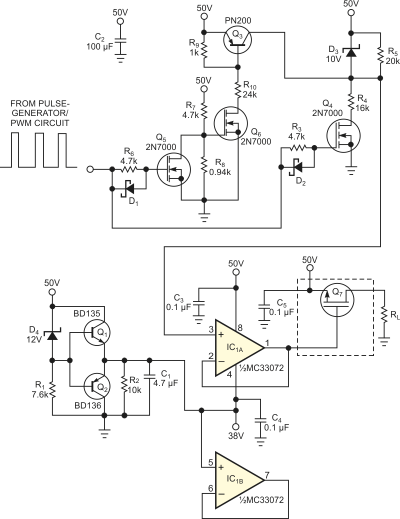
P-channel MOSFETs can simplify designs when you use them as high-side switches on circuits with voltages exceeding 100 V dc. When driving a MOSFET, you must rapidly charge and discharge the input capacitance between its gate and its source to reduce heat losses. The circuit in Figure 1 can accomplish that task. Q7, an International Rectifier IRF5305 power P-channel MOSFET, switches 50 V to a load. A series of pulses from a pulse generator or PWM (pulse-with-modulation) source drives the load at frequencies as high as 60 kHz with a variable duty cycle. The circuit comprises Q4, R5, D2, R4, D3, and R3; provides a means of level-shifting; and ensures that the voltage drop between the gate-to-source of Q7 never exceeds 10 V. When Q4 is on, 10 V develops across D3. This voltage drop turns on Q7 through op amp IC1A, one-half of an MC33072 from ON Semiconductor. IC1A has a 13 V/µsec slew rate and can drive capacitances as high as 10 nF.
 |
||
| Figure 1. | An op amp operating at 38 to 50 V provides power to a load through power-MOSFET Q7. | |
The combination of D4, R1, Q1, Q2, R2, and C1 provides “ground” for the op amp, which is at 38 V – that is, 12 V below the 50 V rail voltage. The positive voltage is 50 V, and ground is 38 V. The anode of D3 connects to the noninverting input of IC1A, whose output drives Q7’s gate at 40 V, which is 10 V below the rail voltage of 50 V. The circuit comprising R6, Q5, D1, R7, R8, Q6, R9, R10, and Q3 rapidly switches D3’s anode to 50 V, which turns off Q7. Transistor Q5 functions as an inverter that turns on Q6, which subsequently drives Q3 to rapidly switch D3’s anode to 50 V and thus drives Q7’s gate. Schottky diodes D1 and D2 alternately enhance the switching speed of Q5 and Q4.
Unity-gain op amp IC1A, with its high slew rate, fast settling, capacitive-driving capability, and feedback of the gate voltage, enhances Q7’s switching speed. Using this circuit, you can achieve a rise time and fall time of approximately 500 nsec at Q7’s output.