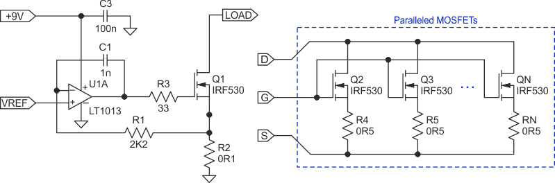
Testing power supplies and batteries requires current loads capable of sinking large current and dissipating substantial amounts of power. A simple but accurate current load can be built using just a single op amp and a power MOSFET, as shown in Figure 1.
 |
||
| Figure 1. | This simple current load and paralleled MOSFETs can be used for larger current and power dissipation. | |
The current through Q1 is derived using this equation:
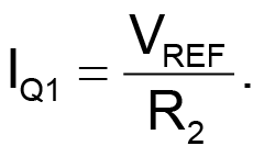 |
(1) |
It can be easily controlled by changing the reference voltage (VREF). The op amp should have low input offset voltage and be capable of operating from a single supply.
If the circuit needs to be capable of sinking large current or dissipating tens of watts, a single op amp can be used to control several MOSFETs operating in parallel. However, simply paralleling MOSFETs creates two unwanted effects. For one thing, the turn-on threshold often varies between transistors (even of the same model), and their thresholds have negative temperature coefficients. This means that there can be a substantial difference between the drain currents in each transistor to begin with, and once a transistor warms up its threshold decreases, further increasing the current and making it even hotter.
To equalize the transistor currents, a small resistor in series with the source of each transistor can be added. For this to be effective the voltage drop across the source resistor must be comparable to the threshold, making it a large fraction of a volt. The consequence is that the equalizing resistors dissipate large power, and the voltage drop across them eats into the minimum voltage at which the circuit can operate.
 |
||
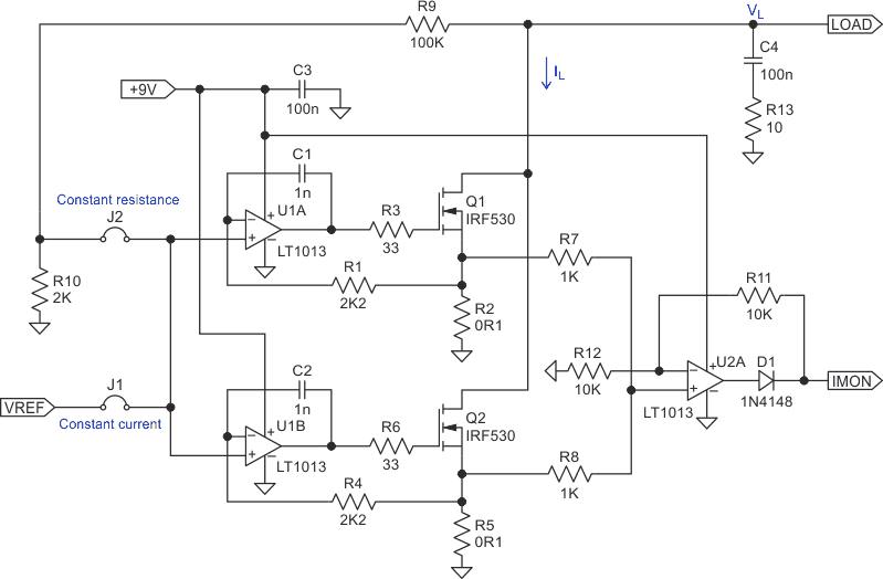
| Figure 2. | This current load schematic uses two independently-controlled MOSFETs. | |
A better way to build a high current, high power load is to control each MOSFET separately, avoiding the current imbalance due to threshold spread. Figure 2 shows two such circuit blocks in parallel, but more can be added if needed. With the jumper J1 closed and J2 open the circuit operates in constant current mode, with the total load current given by:
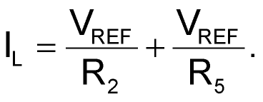 |
(2) |
If the sense resistors are equal (R2 = R5 = RS), the total load current is simply:
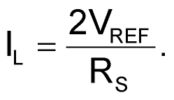 |
(3) |
To measure the total load current, we need to sum up the currents from each transistor, in this case by adding up the voltage drops from all the sense resistors. Usually this is done by an inverting adder followed by an inverter, built with two op amps. The downside is that they need a bipolar power supply due to the voltage inversion at the output of the adder.
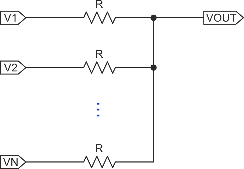 |
||
| Figure 3. | This diagram illustrates the voltage summation at VOUT. | |
In this Design Idea, a simpler way of adding the voltage drops is shown, using the resistors R7 and R8 and just one op amp. The principle of this addition is illustrated in Figure 3. Each of the N resistors is driven by a voltage source with very low impedance, which is what we have when the voltage drops across the sense resistors are applied instead.
If no current is drawn out of the VOUT terminal, from Kirchhoff’s law we have:
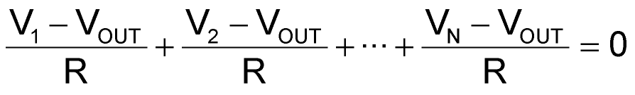 |
(4) |
and therefore
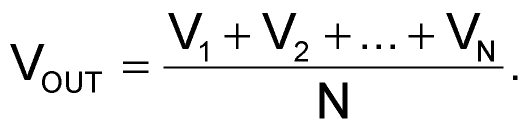 |
(5) |
In the case of two sense resistors, as in Figure 2, the voltage at the non-inverting input of U2A is half the sum of the voltage drops across R2 and R5. After a gain of two by U2A, the output voltage IMON is the sum of the two sense resistor voltages, and can be used to monitor the total load current. The circuit is scalable by adding more basic blocks in parallel, and by using equations 3 and 5 with the number of blocks, we can calculate the total load current and the current sense output before amplification by U2A. Conveniently, one quad op amp can be used with three power blocks.
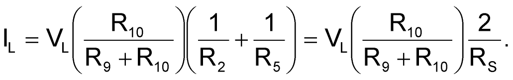
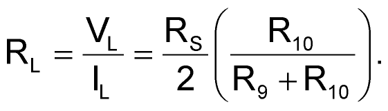
Finally, the current load can be made to behave as a constant resistor, which can be very useful when testing certain power sources. This is achieved by supplying a fraction of the load voltage VL as a reference voltage. With the jumper J2 in (and J1 out), the voltage at the non-inverting inputs of U1A and U1B is determined by VL and the divider formed by R9 and R10, so the load current becomes:
 |
(6) |
From here we can see that the effective load resistance RL is:
 |
(7) |
By adjusting the divider ratio or substituting R10 with a potentiometer, the load resistance can change from the nominal calculated by equation 7 (2.55 Ω for the values in Figure 2) to nearly infinity when R10 = 0.