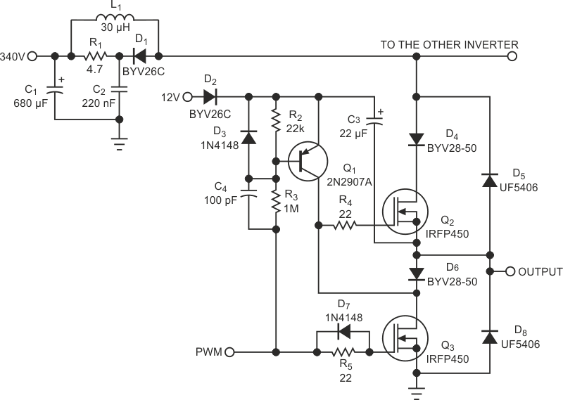
A simple high-voltage MOSFET inverter solves the problem of driving a high-side MOSFET, using a low-voltage transistor, Q1, and a special arrangement involving D6 (Figure 1). This inverter is much faster than those that optocouplers drive, so dead-time problems are minimal. The inverter has the usual blocking diodes D4 and D6, and the parallel diodes D5 and D8. Q3 provides the turn-off signal to Q2. When Q3 turns on, Q2‘s gate short-circuits to ground through R4. R4 limits current and dampens oscillations. Q2‘s gate discharges quickly; only the value of R4 limits discharge time. Q1 stays off, thanks to R2, and C3 charges to 12 V through D2. The gate pulse creates a current through C4, and D3 protects the base-emitter junction of Q1.
 |
||
| Figure 1. | This circuit is probably the simplest high-voltage inverter you can build. | |
In the turn-on of Q2, the following scenario occurs: When the control input, PWM, goes low, Q3 quickly turns off, thanks to D7. A displacement current, C4×dV/dt, flows through C4 to the base of Q1. Q1 charges the output capacitance of Q3 and the gate capacitance of Q2, and Q2 turns on. C3 supplies the collector current. If the period is long, Q1 keeps conducting and compensating the leakage of Q3. If D6 were a Schottky diode, which is leaky, you would have to reduce the value of R1. A short cross-conduction period exists between the two MOSFETs, a phenomenon that is more apparent when Q3 turns off and Q2 turns on. A small inductor, L1, in series with the main supply limits the current spikes. The inductor needs a snubber comprising D1, R1, and C2. Note that the inductor value is conservative and can be smaller.
 |
||
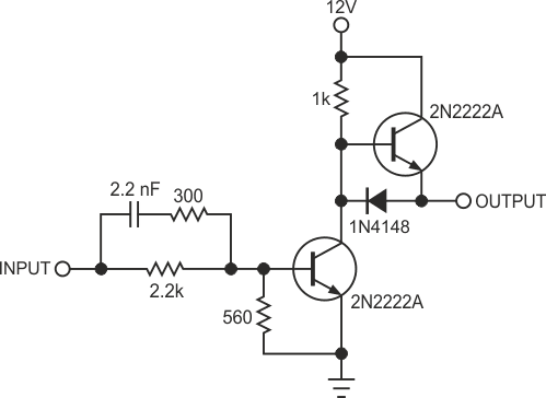
| Figure 2. | his buffer enhances speed at the PWM input of Figure 1’s circuit. | |
The values are for a 370 W, three-phase inverter with 150% overload capacity. If you change the MOSFET, the value of C4 has to change according to the total gate charge plus the output capacitance of Q3, which is much lower and, in fact, negligible. Q1 amplifies the capacitor current, so C4 is proportional to QG2×hFE1. Make C4‘s value no higher than necessary, because the base current in Q1 would be too high. To obtain all the speed advantages of the circuit, the PWM signal should be able to quickly drive Q3. If necessary, you can use a buffer circuit (Figure 2). You can drive the circuit with a single CMOS gate. The circuit in Figure 1 is probably the simplest high-voltage inverter you can design. It has served in thousands of three-phase motor drives from 0.37 to 0.75 kW.