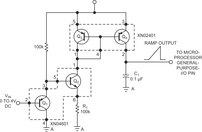
The simple ADC in Figure 1 is perfect for getting analog signals into a purely digital microcontroller. Using just five surface-mount parts, you can assemble it for less than 50 cents (1000), which is approximately half the cost of a single-chip-ADC approach in the same volume. Moreover, this design takes only one pin from the microcontroller to operate. Although you can purchase many microcontrollers with built-in ADCs, in some circumstances, this solution is impractical. For example, you might have an all-digital microcontroller already designed in. In this design, a USB-compatible, digital-only microcontroller needed analog input at low cost for a consumer application. The basic analog portion of the circuit in Figure 1 uses clever transistor arrays from Panasonic. Q1/Q2 and Q3/Q4 are single-package, multiple-transistor arrays. The Q1/Q2 array forms a voltage-to-current converter. The voltage on Q1’s emitter is a diode drop higher than the voltage on Q1’s base. The VBE drop in Q2 returns the original input voltage to the top of R1; R1 then converts that voltage to a current.
 |
||
| Figure 1. | With two transistor arrays and three discrete components, you can configure an analog front end for a microcontroller. |
|
The Q3/Q4 array forms a standard current-mirror circuit. The current flowing in Q3’s collector matches the current forced in Q4’s collector.Q4’s collector has high impedance, so Q4 provides a suitable current source. The current from Q4 charges C1 at a rate that is proportional to the input voltage. The values in Figure 1 allow for a range of conversion times of 3 msec for an input of 4 V to 56 msec for an input of 0.1 V. The design exploits the fact that most general-purpose microcontrollers have a bidirectional I/O-port structure. That is, you can program a port pin as either an input or an output. When you set a pin as an input, it has very high input impedance, so it can follow the ramp as C1 charges up. When you program a pin as an output, you can set it low, and it discharges C1 for the next conversion cycle. This action gives you the basic operation of a single-slope analog-to-digital-conversion cycle. The basic operations are as follows:
- Set the ADC pin as a low output to discharge C1.
- Reset a suitable timer-counter in the microcontroller.
- Set the ADC pin as an input.
- Allow the timer to count until it reads as logic 1 in the microcontroller, or let the timer count to some suitably long value, which suggests that the input is essentially zero.
- Stop the timer counter.
- Convert to the timer count by some suitable scaling factor to an ADC reading.
- Start over for the next conversion.
The conversion from the ramp time to a logic 1 on the microcontroller pin depends on the following factors:
- the logic-1 switching level of your microcontroller;
- the input voltage and, hence, the ramp rate of C1;
- the value of C1, which sets the ramp rate;
- the value of R2, which sets the ramp rate; and
- the microcontroller's timer resolution.
You can boil down these variables to the following equation:
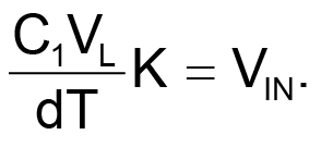
where VL is the voltage level of the microcontroller's zero-to-one conversion, K is the scaling factor that relates to the voltage-to-current conversion of the input stage and timer resolution, and dT is the time count of the conversion cycle. Because C1VL is also a constant for a given circuit, you can combine it with K to form a single conversion constant of K1. Hence, you can reduce the equation to
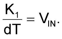
In this case, the test code was written for Microchip Technology's PIC16F84 microcontroller. This device has a measured VL of 1.28 V; the counter has a resolution of 1 µsec. It's probably best to empirically determine the factor K1. Set up the counter resolution as desired, allow the microcontroller to make and display that conversion time or send it through a debugger, and, given that you have an exact VIN, K1 is then easy to determine. In this case, K1 turned out to be 2 V×5700 µsec = 11,400.
The constant K1 serves to convert the raw timer count to a voltage. To obtain high resolution, you normally use floating-point math. If you need to display the value, floating-point math might be appropriate, but most applications entail reading a potentiometer or some other system level. In such applications, the output is a bar-chart display or some control value. Thus, you waste microcontroller resources by using floating-point math throughout the conversion process. With careful selection of circuit components, fixed-point math can usually provide, for example, an 8-bit representation (0 to 255) for an input range of 0 to 4 V. If you scale the timer/counter by 64, instead of a count of 5700 µsec for an input of 2 V, you obtain 89. Then, if you want this 89 to correspond to a half-scale value of 128, the value of K1 becomes 11,392. A 16-bit unsigned word easily accommodates this value, and you need no floating-point math in the conversion. The accuracy of this ADC is approximately 5% with no adjustments. The resolution is a function of the timer resolution and how tight the code makes the conversion loop. The resolution can be many times the absolute accuracy. Moreover, the converter is monotonic.