For some ICs, supply voltages should be applied in a particular sequence. One example is the subscriber line interface circuit (SLIC), which, depending on the application, may require several negative and/or positive voltages. The larger voltages are generally used to ring the phone, and the lower voltages power the phone while it's off-hook.
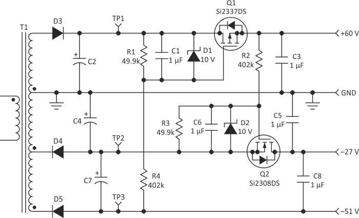
As an example, consider a design that requires output voltages of –51 V, +60 V, and –27 V, all at load currents of several hundred milliamps. The load requires the –51 V to be applied first, followed by the +60 V, and lastly, the –27 V. The transformer secondary windings of a flyback converter provide the three output voltages (Fig. 1). As a result, the output voltages start up together, and it's impossible for one voltage to remain off without affecting the other two.
To achieve the desired startup sequence, the turn-on of the +60-V and –27-V outputs must be delayed. That's accomplished by the additional components in Figure 1. The P-channel FET (Q1) in series with the +60-V rectified output voltage at TP1 holds off the output voltage until the –51 V reaches regulation. Resistors R1 and R4 form a divider between the +60 V and –51 V and are scaled so that Q1's gate-to-source voltage fully enhances Q1 when both the +60 V and –51 V are present. Thus, the parallel combination of R1, R4, and C1 adds a programmable delay before Q1 turns on.
 |
|
| Figure 1. | Adding a pair of FETs and associated components to this typical flyback converter output allows designers to create delays for two of the output voltages. Thus, they can establish a proper turn-on sequence for IC supply voltages. |
The component values in Figure 1 produce a delay of approximately 5 to 10 ms. Since the delay is controlled by the turn-on threshold of the FET, some care must be taken in determining the actual range of the delay time. Zener diode D1 protects Q1 from a gate-to-source over-voltage condition, but could be deleted if desired.
Just as Q1 holds off the +60-V output, Q2 holds off the –27-V output. Q2's gate is controlled by the +60-V switched output voltage. Q2 must be an N-channel FET since the "trigger" voltage applied to the gate to turn it on is positive-going rather than negative-going, as is the case with Q1.
Some care must be taken when using this technique. While Q1 and Q2 are in their off state, the output voltages at TP1 and TP2 become unloaded. This may cause the rectified voltages to overshoot by peak-detecting voltage spikes. The spikes are typically due to the transformer's leakage inductance. This effect can be minimized by adding snubbers across the diodes or by adding preload resistors in parallel with the output capacitors.
Also, the drain-to-source voltage drops across Q1 and Q2 increase as the load current rises. Therefore, increased loading degrades voltage regulation if the FETs don't have a low RDS(ON). This circuit works best with output voltages above 10 V and load currents below 0.5 A, so the FET voltage drops are negligible.
The output voltage turn-off sequencing depends on the loading placed on the outputs during power-down. Any output with a sufficiently large load will collapse the voltage quickly. That's because there's only a fixed amount of energy storage available in the output capacitors. This circuit can be added to any set of power-supply outputs with large enough voltage differentials between them.